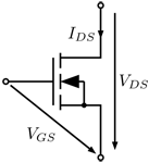
MOSFET  -
- characteristics
Just skip this information and continue with the plot anyway, this help may be shown by clicking the -icon.
This application plots the - characteristics of a n-channel MOSFET according to the
input data characterizing the transistor and its functional state.
How to use this application
On the right side of the screen the desired settings may be inputted. On changing a value, the plot on the left side automatically changes by recalculating the transistor equations described below. More than one curve parametrized by the gate-source voltage may be plotted at once. To access this help click the -icon in the top right corner. It may be closed by clicking here or by using the close label in the top right corner of this overlay.
MOSFET drain current
The formula for the drain current is derived with the
gradual channel approximation. This model assumes a voltage drop across the channel caused by the outer drain-source voltage which shrinks the conducting channel limiting the current. This approximation leads to the following formula:

with

containing the transistor's geometry and material properties.  is the threshold voltage of the transistor describing the minimum gate voltage for strong inversion and thus starting to conduct:

Note that in the formula above the intrinsic carrier concentration is temperature dependent as well. This application correctly consideres this fact, so no action has to be taken by the user when changing temperature.
The formula for above describes an upside down parabola. Experiments show that the drain current does not decrease as the formula suggests when gets bigger and bigger.
If gets bigger than the so called saturation voltage (which is the drain-source voltage at the maximum drain current), the transistor is said to be in saturation. Otherwise it's said to be in linear operation. In saturation, the current through the transistor can not be increased by an increase in drain source voltage.
It basically acts as a voltage controlled current source. The current drive of the transistor in the saturation region can be calculated with the following equation:

Note the extra term with  inside. This quantity is called the channel length modulation coefficient.
Experiments show that the drain current slightly increases when increasing the drain-source voltage in saturation. So a MOSFET is not an ideal current source, as the current is dependent on the voltage applied. To regard this fact in the formula, this coefficient was introduced. When being zero, the transistor acts like an ideal current source. This value may only be determined experimentially, typical values lie between 0.0001V-1 and 0.1V-1.
inside. This quantity is called the channel length modulation coefficient.
Experiments show that the drain current slightly increases when increasing the drain-source voltage in saturation. So a MOSFET is not an ideal current source, as the current is dependent on the voltage applied. To regard this fact in the formula, this coefficient was introduced. When being zero, the transistor acts like an ideal current source. This value may only be determined experimentially, typical values lie between 0.0001V-1 and 0.1V-1.
Parameters

- K
- If selected, the value of .
- Z
- The width of the transistor (only applies if is calculated).
- L
- The gate length of the transistor (only applies if is calculated).
- μn
- The electron mobility of the transistor substrate (only applies if is calculated).
- Cox
- The specific capacitance of the gate oxide (only applies if is calculated).
- : threshold voltage
- Vth
- If selected, the value of .
- tox
- The width of the gate oxide (only applies if is calculated).
- εox
- The relative permettivity of the gate oxide (only applies if is calculated).
- NA
- The acceptor doping concentration (only applies if is calculated).
- ni
- The intrinsic carrier concentration of the substrate at 300K (only applies if is calculated).
- T
- The temperature (only applies if is calculated).
- VFB
- The flat band voltage of the transistor (only applies if is calculated).
- : channel length modulation
- λ
- The channel length modulation.
 : gate-source voltage
 - VGS
- The gate source voltage. To plot more than one gate voltage, add another one with the ⊕-button.