An IGBT is a combination of an insulated gate FET and a bipolar transistor. It is primarily used for switching high power loads
The bulk of the device is the $n^-$-region called the drift region. In order to sustain a large voltage drop across the device it is lightly doped and wide. In the on-state, the conductivity is increased by electrons injected from the $n^+$ region and holes injected from the $p^+$ region.
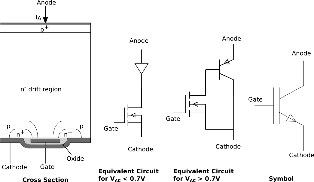
When a voltage $V_{GC}$ above the threshold voltage is applied to the gate, a conductive channel is formed connecting the $n^-$ and $n^+$ regions. Depending on the value of $V_{AC}$ three modes of operation can be observed. With a small $V_{AC} < 0.7V$ the equivalent circuit is that of a MOS transistor in series with an PN-Diode under forward bias. Since the voltage drop across the MOS transistor can be neglected, the current is roughly that of a PN-Diode under forward bias:
\[ \begin{equation} I_A \approx \frac{4Aen_iD_A}{x_{nn}}\exp\left(\frac{eV_{CE}}{2kT}\right) \end{equation} \]Here $D_A$ is the ambipolar diffusion coefficient which is defined as: $D_A=\frac{n_n+p_n}{n_n/D_p + p_n/D_n}$ and $x_{nn}$ is the neutral drift region (Sze page 93).
The second regime starts with $V_{AC} > 0.7V$ where the characteristics resemble those of a MOSFET. Not all holes injected from the $p^+$ region can recombine in the $n^-$ layer and thus contribute to a pnp bipolar current. The MOSFET current $I_{MOS}$ becomes the base current of the pnp bipolar transistor. Therefore the total current is the sum of the MOS current and the pnp current, which is the MOS current amplified by the pnp transistors current gain $\beta_{pnp}$
\[ \begin{equation} I_A = I_{MOS} + I_{C,pnp} = (1+\beta_{pnp})I_{MOS} \end{equation} \]The MOS current in the linear regime $(V_{DS} < V_{sat}=V_G-V_T)$ can be calculated with:
\[ \begin{equation} I_{MOS} = \frac{W}{L}\mu_mC_{ox}[V_G-V_T-\frac{V_{DS}}{2}]V_{DS} \end{equation} \]And for the saturation regime $(V_{DS} > V_{sat}=V_G-V_T)$
\[ \begin{equation} I_{MOS} = \frac{W}{2L}\mu_mC_{ox}(V_G-V_T)^2 \end{equation} \]An important thing to note here is that the Drain-Source voltage $V_{DS}$ of the MOS transistor is the Anode-Cathode voltage minus the voltage drop of the emitter-base Diode of the pnp transistor. For the following diagram it is assumed that the voltage drop is constant but in reality it would also vary with current through the device.
\[ \begin{equation} V_{DS}=V_{AC}-V_{EB,pnp} \approx V_{AC}-0.7V \end{equation} \]The pnp current gain $\beta_{pnp}$ can be calculated from the base transport factor $\alpha_T$
\[ \begin{equation} \beta_{pnp}=\frac{\alpha}{1-\alpha} \end{equation} \] \[ \begin{equation} \alpha\approx\alpha_T\approx\frac{1}{\cosh(x_{nn}/L_n)} \end{equation} \]Here $x_{nn}$ is the neutral with of the pnp base region and $L_n$ the diffusion length.
$\beta_{pnp}$ is usually around unity, meaning that electron and hole current have a similar magnitude. But compared to a comparable power MOSFET the current and transconductance $g_m$ are doubled. This is the main advantage of an IGBT.
Since there is also a parasitic bipolar npn transistor in parallel with the MOSFET, there exists an third operating regime when the product of $\beta_{pnp}*\beta_{npn}$ becomes > 1 and the IGBT latches into an constant on state similar to a thyristor. If this is the case the current $I_A$ through the device can not be controlled with the gate voltage anymore and therefore this regime should be strictly avoided. Modern IGBT devices try to minimize this effect through various means.
IGBTs combine the high gate impedance of an MOSFET with the low saturation voltage and high current capabilities of an bipolar transistor. Because of this they are often used in medium and high power applications such as switched-mode power supplies, motor controllers and induction heating.
One disadvantage of IGBTs is that there is a lot of charge stored in the $n^-$ region. Because of that, after turn-off, a tail current exists that decays exponentially, roughly with the minority carrier lifetime. Typically it lasts around 10-50 ms which limits the switching speed of an IGBT to less than 10 kHz. This effect can be reduced e.g. by putting a $n^+$ region in between the collector $p^+$ region and the $n^-$ region in order to absorb the holes quickly. But as a downside this increases the voltage drop across the pn-junction.
|
Reference: Physics of Semiconductor Devices, S. M. Sze, Chapter 11
Wikipedia