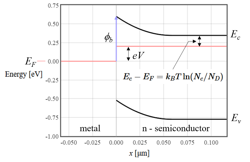
A Schottky contacts form at the interface between a metal and a semiconductor. At the interface, there is usually a high concentration of interface states that put the Fermi energy about in the middle of the band gap of the semiconductor. The exact position of the Fermi energy depends on the materials involved and how the metal-semiconductor interface was prepared. Since the Fermi energy is near the center of the band gap, the semiconductor is depleted of mobile charge carriers near the interface. In a Schottky contact, this depleted region is too wide for the electrons to tunnel through, so only the charge carriers that have enough thermal energy to go over the barrier.
Every electron state in a crystal can be assigned to a wave vector $\vec{k}$. The electrical current density can be calculated as a sum over the occupied electron states,
$$\vec{j}= -e\int \vec{v}_{\vec{k}}D(\vec{k})f(\vec{k})d^3k,$$where $e$ is the elementary charge, $D(\vec{k}) = \frac{2}{(2\pi)^3}$ is the density of states in $\vec{k}$, $\vec{v}_{\vec{k}}$ is the group velocity of state $\vec{k}$, and $f(\vec{k})$ tells us the probability that the $\vec{k}$ state is occupied. In equilibrium, the probability that a state is occupied is given by the Fermi function. We will assume that we are close enough to equilibrium that we can use the Fermi function to describe the occupation of the $\vec{k}$ states. The group velocity is,
$$\vec{v}_{\vec{k}} = \frac{\nabla_{\vec{k}}E(\vec{k})}{\hbar},$$where $E(\vec{k})$ is the electronic band structure. For a more detailed discussion of calculating electron current densities, see the transport section of the Advanced Solid State Physics course.
For simplicity, we assume that the conduction band can be described by a single effective mass. The energies of the $\vec{k}$ states in the conduction band are
$$E = E_c + \frac{\hbar^2k^2}{2m^*},$$where $E_c$ is the conduction band edge and $m^*$ is the effective mass. Taking the gradient of the band structure gives the group velocity,
$$\vec{v}_{\vec{k}} = \frac{\hbar}{m^*}\left(k_z\hat{x}+k_y\hat{y}+k_z\hat{z}\right).$$The current density can then be written as,
$$\vec{j}= \frac{-e\hbar}{4\pi^3m}\int \left(k_x\hat{x}+k_y\hat{y}+k_z\hat{z}\right)f(\vec{k})d^3k.$$We define the interface between the metal and the semiconductor as the $x=0$ plane. The region where $x < 0$ is the metal, and the region where $x > 0$ is an n-type semiconductor. By symmetry, the $y-$ and $z-$components of the current density must be zero. There is only a current flowing perpendicular to the $x = 0$ plane.
$$j_x = \frac{-e\hbar}{4\pi^3m}\int k_x f(\vec{k})d^3k.$$At zero bias voltage, there must be zero current. Some of the electrons in the metal have enough thermal energy to get over the Schottky barrier to the semiconductor, but there are electrons in the semiconductor with enough energy to go over the barrier in the other direction. We consider the case where a voltage is applied to lift the energies of the electrons in the semiconductor. Now, many more electrons have enough energy to get over the barrier from the semiconducting side to the metal. The electrons in the metal still see the same barrier, so there is no increase in the number of electrons going from the metal to the semiconductor. We will now estimate the number of electrons going from the semiconductor to the metal under these forward bias conditions.
Assign the Fermi energy on the metal side to an energy of zero. In that case, the Fermi energy on the semiconductor side is $eV$. The energy of the electrons in the semiconductor is,
$$E = E_c+\frac{\hbar^2k^2}{2m^*} = eV + k_BT\ln (N_c/N_D)+\frac{\hbar^2k^2}{2m^*}.$$
The electrons that go over the Schottky barrier have an energy more than $3k_BT$ higher than the Fermi energy of the semiconductor, so the Boltzmann approximation can be used and the Fermi function is approximated by, $f(E) \approx \exp\left(\frac{E_F - E}{k_BT}\right)$. Substituting $eV$ for $E_F$ and using the expression of the electron energy yields,
$$f(E) \approx \exp\left(\frac{-k_BT\ln (N_c/N_D)-\frac{\hbar^2k^2}{2m^*}}{k_BT}\right),$$and the current density becomes,
$$j_{s \to m}= \frac{-e\hbar}{4\pi^3m^*}\int k_z\exp\left(\frac{-k_BT\ln (N_c/N_D)-\hbar^2k^2/2m}{k_BT}\right)d^3k.$$A factor of $N_D/N_C$ can be pulled out of the integral. The remaining part has to be integrated over $k_x$, $k_y$, and $k_z$.
$$j_{s \to m}= \frac{-e\hbar}{4\pi^3m^*}\frac{N_D}{N_c}\int k_x\exp\left(\frac{-\hbar^2k^2}{2mk_BT}\right)dk_xdk_ydk_z.$$The integrals over $k_y$, and $k_z$ each yield a factor of $\sqrt{\frac{2\pi m^*k_BT}{\hbar^2}}$ because $\int\limits_{-\infty}^{\infty}\exp(-ax^2)dx = \sqrt{\frac{\pi}{a}}$.
The remaining integral over $k_x$ has to be integrated just over the wave vectors that have enough energy to get over the barrier, which is given by the condition, $\phi_b = eV + k_BT\ln (N_c/N_D)+\frac{\hbar^2k_c^2}{2m^*}$. There is a subtle minus sign at this point. The electrons are moving in the $-x$ direction, so the electrons that go over the barrier all have negative $\vec{k}$ vectors. The integral is, $$j_{s \to m}= \frac{-ek_BT}{2\pi^2\hbar}\frac{N_D}{N_c}\int\limits_{-\infty}^{-k_c}k_x\exp\left(\frac{-\hbar^2k^2}{2mk_BT}\right)dk_x.$$
Using the identity,
$$\int\limits_{-\infty}^{-k_c}k\exp (-ak^2)dk = -\frac{\exp(-ak_c^2)}{2a}$$the current density is,
$$j_{s \to m}= \frac{em^*k_B^2}{2\pi^2\hbar^3}T^2\frac{N_D}{N_c}\exp\left(-\frac{\phi_b-eV -k_BT\ln(N_c/N_D)}{k_BT}\right).$$This simplifies to,
$$j_{s \to m}= \frac{em^*k_B^2}{2\pi^2\hbar^3}T^2\exp\left(-\frac{\phi_b}{k_BT}\right)\exp\left(\frac{eV }{k_BT}\right).$$Using the condition that the current density must go to zero at zero applied voltage, the final expression for the current is,
$$I = \frac{Aem^*k_B^2}{2\pi^2\hbar^3}T^2\exp\left(-\frac{\phi_b}{k_BT}\right)\left(\exp\left(\frac{eV }{k_BT}\right)-1\right),$$where $A$ is the area of the Schottky diode. This has the same form as the diode current for an ideal pn diode, $I=I_s\left(\exp\left(\frac{eV}{k_BT}\right)-1\right)$, however, the saturation current $I_s$ has a different temperature dependence for a Schottky diode than for a pn diode. In this derivation, the current was calculated assuming a forward bias, and it agrees well with experiment in forward bias. Measurements of the saturation current in reverse bias may be orders of magnitude different from what this model predicts.