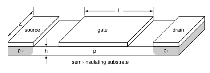
The expression for the drain current in the linear region of a p-channel MESFET is,
\[ \begin{equation} I_D=I_p\left[\frac{V_D}{V_p}-\frac{2}{3}\left(\frac{V_G+V_D+V_{bi}}{V_p}\right)^{3/2}+\frac{2}{3}\left(\frac{V_G+V_{bi}}{V_p}\right)^{3/2}\right], \end{equation} \]where,
\begin{align} I_p =-\frac{\mu_n {N_A}^2 Z e^2 a^3}{2L\epsilon} \qquad V_p = -\frac{e {N_A} a^2}{2 \epsilon} \qquad V_{bi}=\frac{\phi_b-k_BT\ln\left(\frac{N_v(T)}{N_A}\right)}{e}. \end{align}Here $\phi_b$ is the Schottky barrier height. It is the energy difference between the Fermi energy of the metal and the valence band of the semiconductor at the interface. The Schottky barrier depends on the workfunctions of the materials and also on the interface states which tend to pin the Fermi energy to the middle of the band gap.
The linear region is defined as:
\begin{align} V_{DS} < 0 \qquad V_{DS} > V_{DSsat} \qquad V_{DSsat} = -V_p - V_{bi} - V_G \end{align}If $V_D < V_{DSsat}$, then the MESFET is in saturation.
|
$V_{bi}=$ V; $I_p=$ mA; $V_p=$ V.