Problem 1
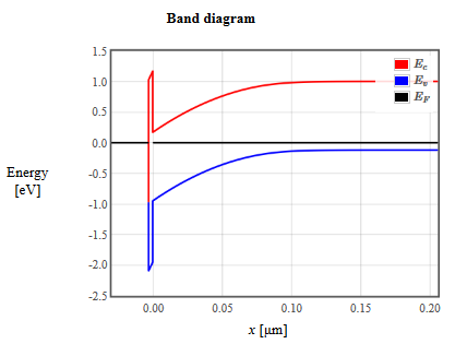
Consider a n-channel MOSFET (with a p-type body) in weak inversion. The electron concentration near the semiconductor-oxide interface is smaller than the acceptor doping in weak inversion. The band diagram is shown below.

(a) Draw the charge densities: the electron concentration $n$, the hole concentration $p$, and the total charge density $\rho$. Draw a line on the charge density axis to indicate the acceptor concentration $N_A$.
(b) Draw the electric field that corresponds to this band diagram.
Problem 2
(a) Draw a $p$-channel MESFET indicating where the depletion layer would be at zero bias. Draw Ohmic contacts at the source and drain.
(b) What is pinch-off?
(c) To achieve pinch-off, should VGS be positive or negative? Why?
(d) What is the primary mechanism that causes the current flow from gate to source? Drift, diffusion, thermionic emission, or tunneling?
(e) What is the primary mechanism that causes the current flow from source to drain? Drift, diffusion, thermionic emission, or tunneling?
(f) Draw the ID vs. VDS for various values of the gate voltage.
Problem 3
Consider a pnp bipolar transistor in a common base configuration. The base is at zero potential.
(a) Draw the band diagram (valence band, conduction band, Fermi energy) assuming no voltage bias is applied.
(b) Draw the electric field also assuming that no voltages are applied.
(c) A current $I_E=1\,\text{mA}$ flows from the emitter to the base. Plot the collector current for positive and negative voltages at the collector. Mark the current axis in mA. Indicate where the transistor is in the forward active region, saturation, and/or cut-off.
(d) If $I_E=0$ and light falls on the transistor, how will the light affect the collector current? Does the wavelength of the light matter?
Problem 4
(a) Draw the depletion widths and the minority carrier concentrations in a pnpn thyristor in forward blocking mode.
Quantity | Symbol | Value | Units | |
| electron charge | e | 1.60217733 × 10⁻¹⁹ | C | |
| speed of light | c | 2.99792458 × 10⁸ | m/s | |
| Planck's constant | h | 6.6260755 × 10⁻³⁴ | J s | |
| reduced Planck's constant | $\hbar$ | 1.05457266 × 10⁻³⁴ | J s | |
| Boltzmann's constant | kB | 1.380658 × 10⁻²³ | J/K | |
| electron mass | me | 9.1093897 × 10⁻³¹ | kg | |
| Stefan-Boltzmann constant | σ | 5.67051 × 10⁻⁸ | W m-2 K-4 | |
| Bohr radius | a0 | 0.529177249 × 10⁻¹⁰ | m | |
| atomic mass constant | mu | 1.6605402 × 10⁻²⁷ | kg | |
| permeability of vacuum | μ0 | 4π × 10-7 | N A-2 | |
| permittivity of vacuum | ε0 | 8.854187817 × 10⁻¹² | F m-1 | |
| Avogado's constant | NA | 6.0221367 × 10²³ | mol-1 |