Problem 1
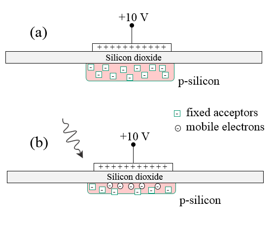
A positive voltage is applied to the gate of a MOS capacitor. This depletes the region under the gate as in figure (a).

(a) Draw the band diagram (conduction band, valence band, Fermi energy) along a line going from the metal across the oxide into the semiconductor. The p-type semiconductor is in depletion.
(b) Draw the electric field and the charge density.
(c) Light falls on this device and mobile electrons are collected at the silicon/oxide interface as in figure (b). Draw the electric field and the charge density for this situation.
Problem 2
(a) Draw an n-channel JFET.
(b) Explain how a JFET works.
(c) Where are there tunnel contacts in this device? What is the purpose of tunnel contacts? Draw the band diagram (valence band, conduction band, Fermi energy) of a tunnel contact.
(d) Why is a JFET slower than a MESFET?
Problem 3
(a) Draw an $p$-channel MOSFET showing the source, drain, gate, and body contacts.
(b) How should this MOSFET be biased so that it is in the saturation regime?
(c) A voltage is applied between the source and the body that reverse biases the source-body junction. Explain how this shifts the threshold voltage. Which direction is the threshold voltage shifted and how far can it be shifted?
(d) Explain what latch-up is in CMOS circuits.
Problem 4
In a silicon $pnp$ bipolar transistor, the emitter is doped to 1019 cm-3, the base is doped to 1014 cm-3, and the collector is doped to 1013 cm-3.
(a) Why is the transistor doped this way?
(b) What is the equilibrium concentration of minority carriers in the collector?
(c) How can you calculate the collector current?