A laser diode is a diode that, when forward biased, emits an intense, coherent beam of light (laser beam). As for LEDs, direct band gap compound semiconductors are used to fabricate laser diodes. The color of the emitted light is determined by the width of the band gap. Below a certain threshold voltage a laser diode behaves in principle like a conventional LED: Carriers (electrons and holes) get injected into the depletion region where they can recombine and emit a photon with a wavelength corresponding to the band gap (spontaneous emission). As soon as the applied voltage is higher than the threshold voltage stimulated emission sets in. As in other lasers an optical cavity is needed to achieve population inversion and thus high enough gain to work as a laser. In the simplest case this cavity is formed by an optical waveguide which confines the light to a narrow region and perfectly parallel cleaved edges of the crystal which then work as a resonator. Additional information about laser diodes can be found at: Laser diode - Wikipedia and electrical4u - laser diodes.
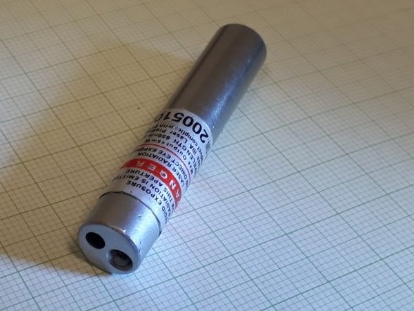
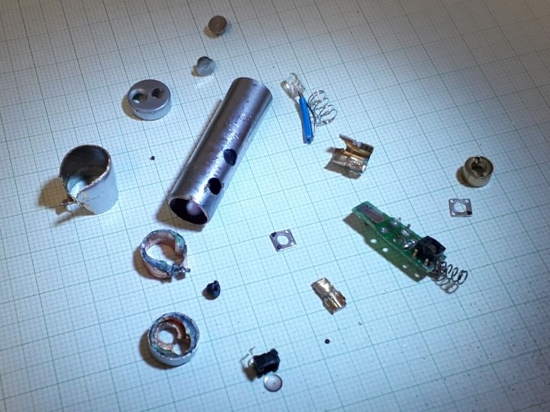
An old laser pointer was disassembled to dismount and investigate its laser diode. A pipe cutter was used to cut open the package and pliers to dismount the individual parts. The chip containing the laser diode was then put into a Scanning Electron Microscope (JEOL JSM-6490LV). The following pictures show different steps of the decapsulation and first overview SEM images of the laser diode.
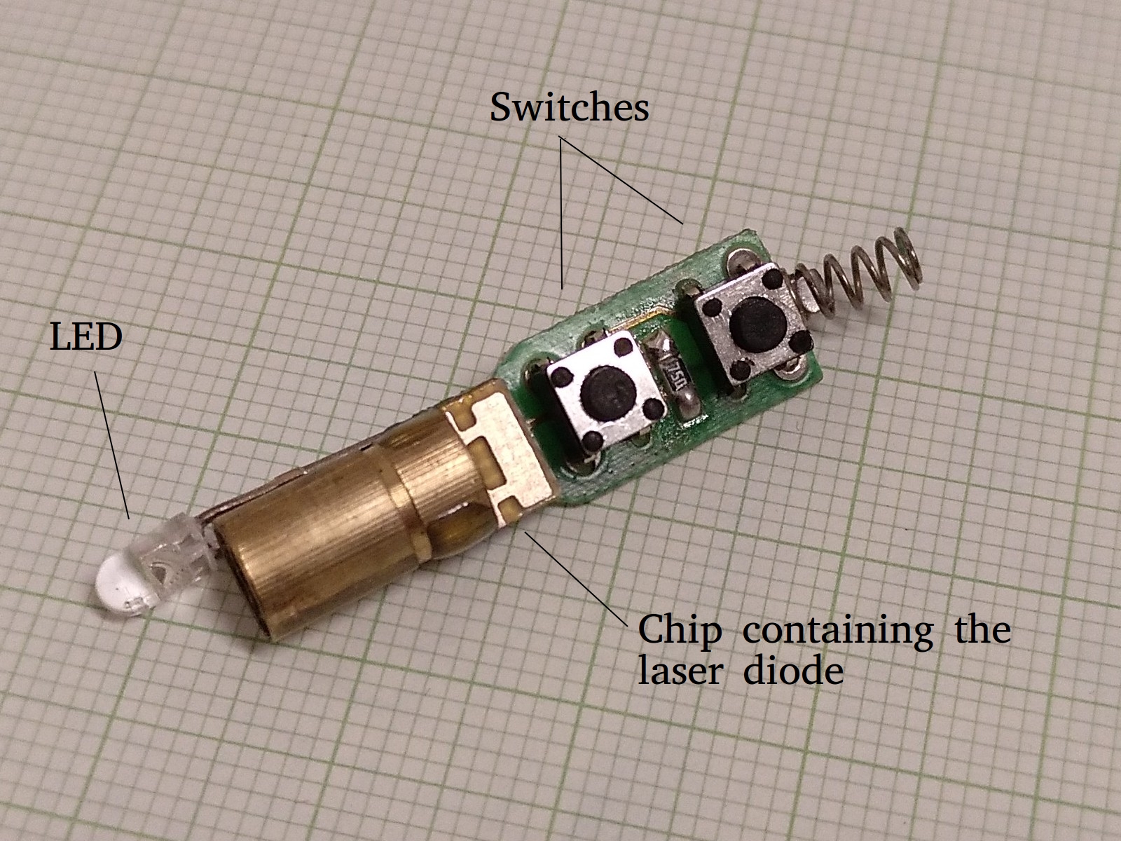
First row from left to right: The laser pointer; all parts after opening the package; the circuit board including the laser diode chip, an LED and the switches.
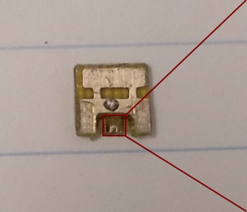
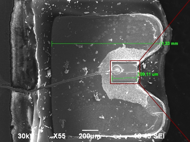
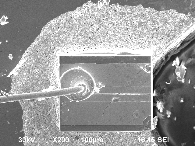
Second row from left to right: Circuit board containing the laser diode chip; SEM image of the laser diode chip showing the dimensions of the chip and of the actual laser diode; laser diode crystal (dimensions: ~310 × 250 μm) the bottom contact was established using a conductive paste, the top contact via a wire bond.
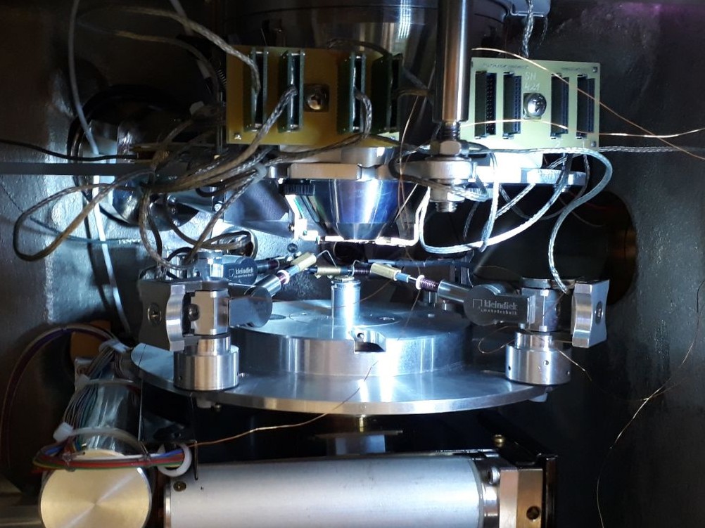
In order to perform electrical measurements the laser diode was contacted using a micromanipulator with two conductive tips inside the SEM. The tips were connected to a Keithley 2636A Sourcemeter One tip was placed on the wire on top of the laser diode, the other tip was placed at the bottom onto the conductive paste. The position of the tips had be carefully adjusted to advoid contact problems but thereafter good measurements could be achieved.
The following images show the micromanipulators inside the SEM chamber and a SEM micrograph of the laser diode with one of the probe tips on the bottom contact.
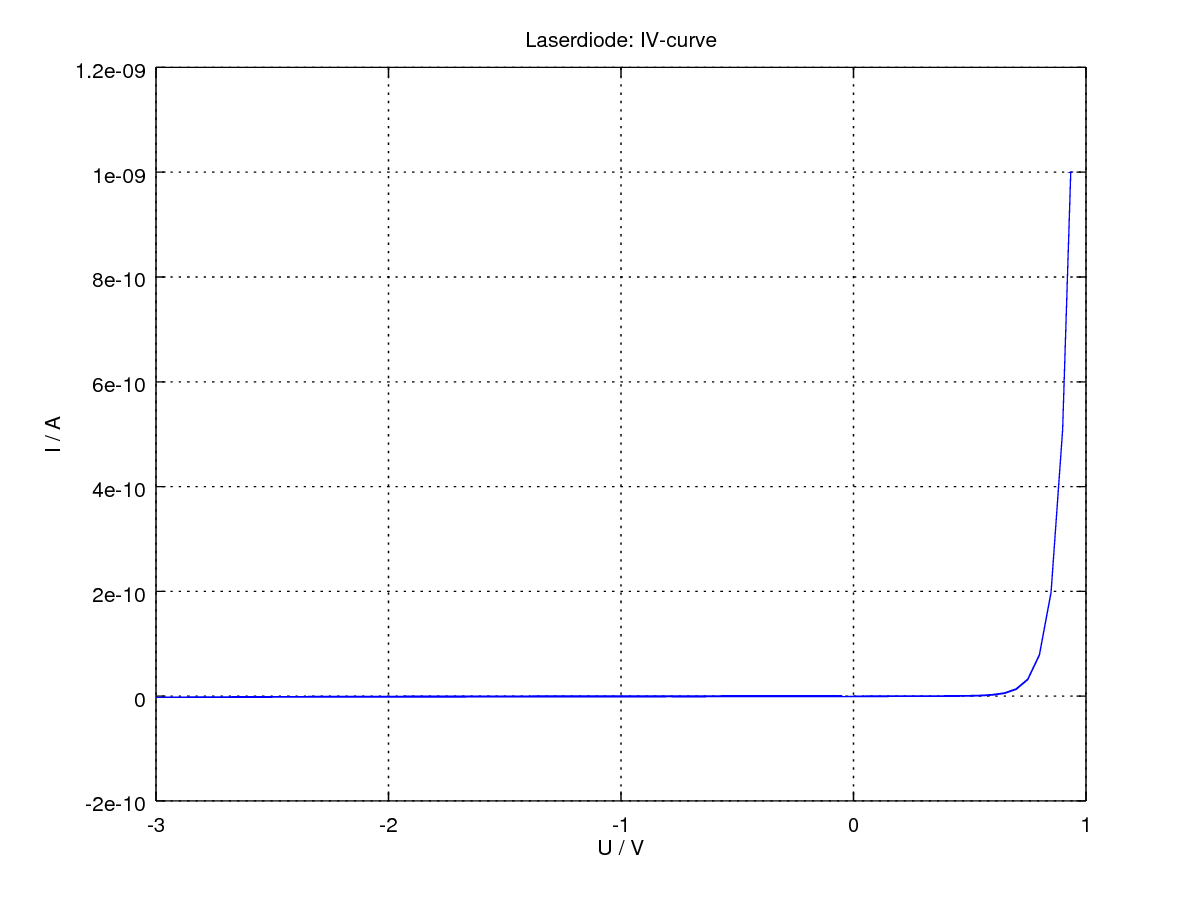
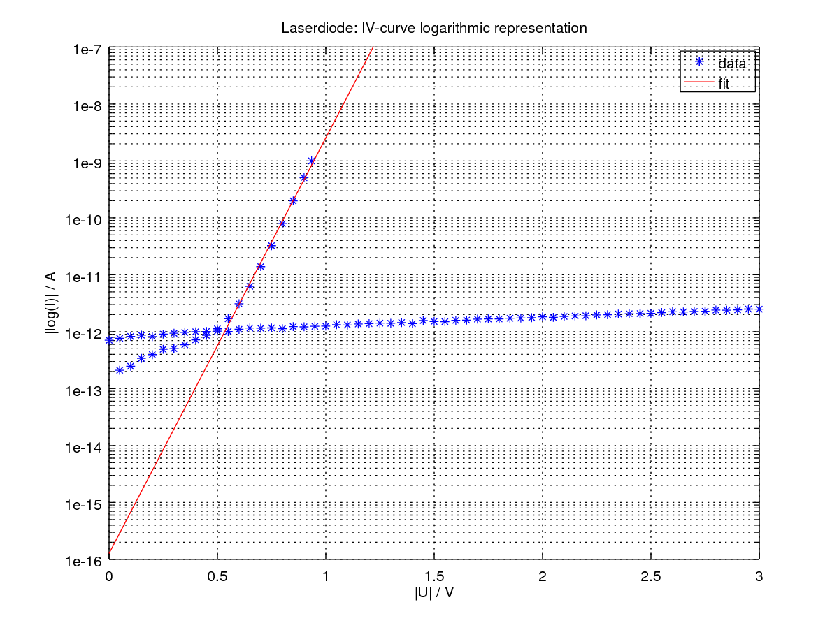
The I-V-curves were recorded with the help of the Python scripts smu-DiodeSweep_test and smu_DiodeSweep_log. During the measurements the electron beam of the SEM was blanked since it would influence the behaviour of the junction. Since it is known that the grounded tip was on the bottom of the laser diode and the biased tip on top, it can be seen from the IV-curve that the upper layer of the laser diode is p-doped, the bottom is n-doped. From the logarithmic plot one sees that the saturation current in reverse bias amounts to approximately Isat,rev ~ 10-12 A and that it is not really stable with increasing voltage. The saturation current in forward bias (which should equal the saturation current in reverse bias) was calculated via the simplified ideal diode equation (s. Diode equations) and a linear fit through the measured data and yields Isat,for ~ 1.3 × 10⁻¹⁶ A. This implies that either the measurement range was chosen wrong so that the saturation current in reverse bias was not measured correctly or the idealized diode equation does not describe the measured device correctly.
A CV-curve was recorded to investigate the capacitic behaviour of the laser diode using the following setup: The n-side of the diode was connected to the sine-wave output of the Lock-In Amplifier (Stanford Research System SR830 DSP) and the p-side to the low noise current preamplifier (Stanford Research System SR570) which was then again connected to the input of the Lock-In Amplifier. The curve was recorded using the CVprofiling python script.
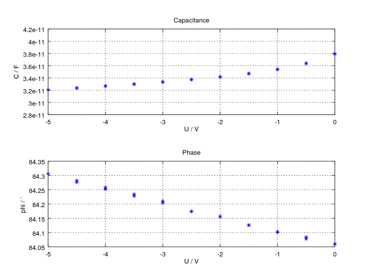
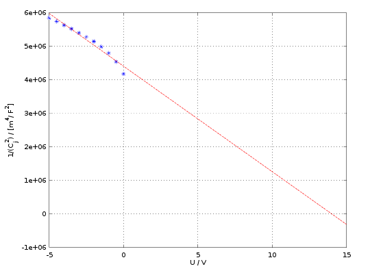
The left image shows the capacitance (top) and the phase shift (bottom) of the the laserdiode as a function of voltage. The right image shows \( 1/C^2_j \) with the specific capacitance \(C_j\) ( = capacitance divided by the active area which was approximated via the dimensions of the chip, compare also to the EBIC images further below) as a function of the voltage. The intersection of the linear fit with the \(x\)-axis should yield the built-in voltage of the junction. However, the obtained value of about 14 V seems not quite realistic.
To investigate which areas of the laser diode are active, EBIC images (= Electron Beam Induced Current) were recorded. EBIC works on basis of the generation of electron hole pairs in a semiconductor due to the irradiation with the electron beam of the SEM. The electron hole pairs get separated due to the built in electric field in a pn-junction and thus a current can be measured. Due to the small size of the electron beam and via a synchronization of the position of the beam and the measured current lateral resolved current measurements are possible. For further information see EBIC on Wikipedia.
To perform this measurements, one side of the diode was grounded, the other connected to a low noise current amplifier. After changing the signal from digital to analogue it was fed into ADwin-ProII, which ran to the computer on which the measurements were controlled with the program Python Ebic2D-SE. The results show that the whole device is active, with the whole toplayer being a p-type semiconductor (known from the IV measurements s. above).
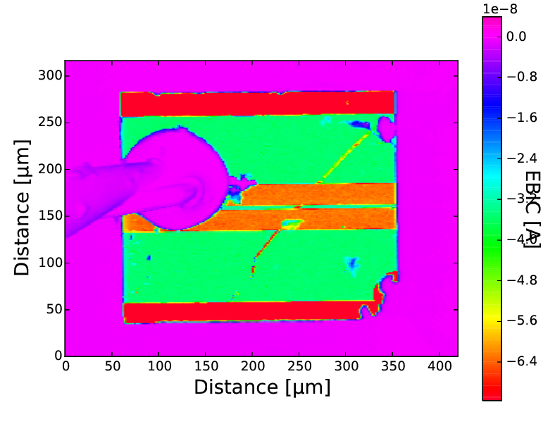
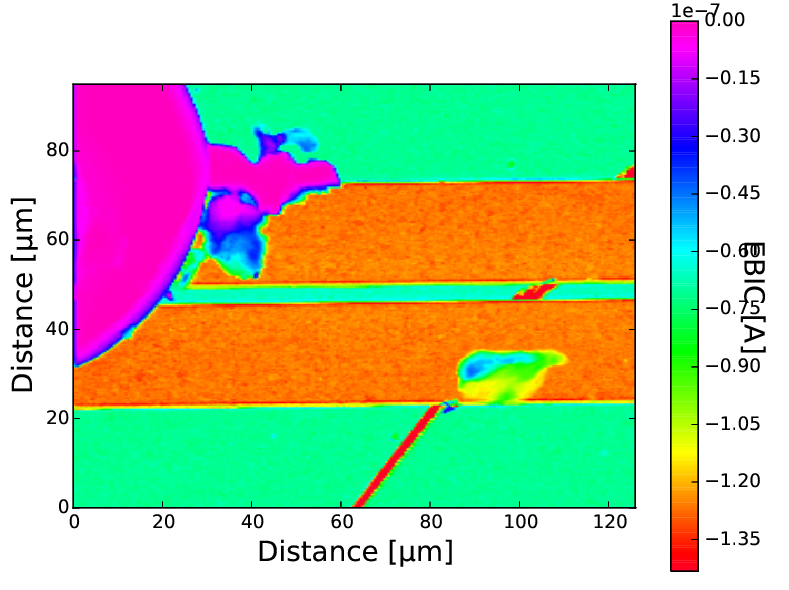
The left image shows an EBIC of the whole chip, the right a close up of the inner part. The green part in the images corresponds to some thin metal top layer (most probably gold) which shields the semiconductor below. The two orange channels show a higher induced current than the other parts which either means that these channels have a thinner metal cover or are electrically more active. The red (=higher current) edges of the chip in the left picture show a region of the semiconductor that is not covered by a metal, thus the electron beam is not screened.
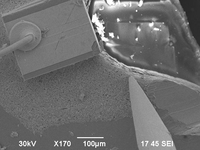
After the EBIC measurements SEM images of the cross section of the laser diode were be recorded.
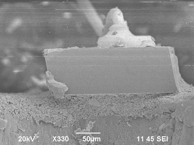
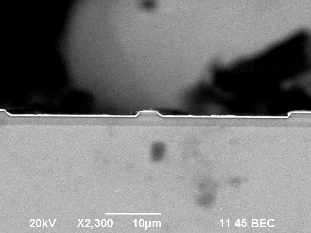
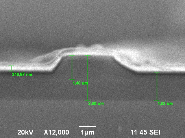
From left to right: SE image of the whole semiconducting crystal, the substrate and the wire bond; BSE image of the cross section beneath the channels; close up SE image of the area between the channels including thickness measurements of the individual layers.
The SEM images of the cross section show that the upper, p-doped part of the crystal is only a few microns (1.8-2.6 μm) thick whereas the whole lower part of the crystal is n-doped. This implies that during the manufacturing a n-doped substrate was used on which the p-doped layer was grown or implanted and on top of that a metal layer was deposited. Having a close look on the right image one observes a slight contrast change in the protruding area between the channels which might possibly correspond to a third differently doped layer in this area. Based on the EBIC images and the SEM images of the cross section we assume that the real active, light emitting part of the laser diode is only the small area between the channels.