Scanning Electron Microscopes (SEMs) create images by shooting
electron beams onto probe surfaces. For every pixel on the final picture
this must be done. The goal of the following experiments
was to analyze the effect of said electron beams on the output characteristics
of semiconductor devices, specifically on a diode and a MOSFET operated as a diode. As electron
beams provide additional charge carriers, measurable changes of the measured currents in the
output characteristics were expected.
Measurement on a MOSFET
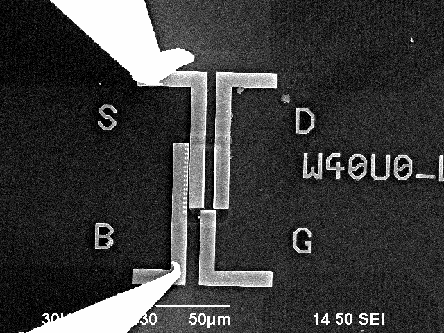
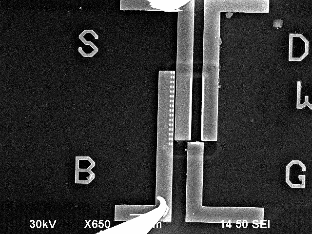
The SEM was used to find a suitable MOSFET on the surface of a chip. The
measurements were conducted via a sourcemeter connected to the SEM. Image
1 shows the setup for the measurement on the MOSFET. The two measuring
pins were attached to the base and the source to operate the MOSFET as a diode. Fig. 1: MOSFET on the Chip surface with two measuring pins attached.
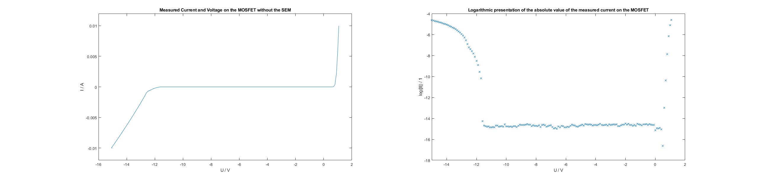
The output characteristic was measured by
conducting a voltage sweep with the currents limited from -10 mA to 10
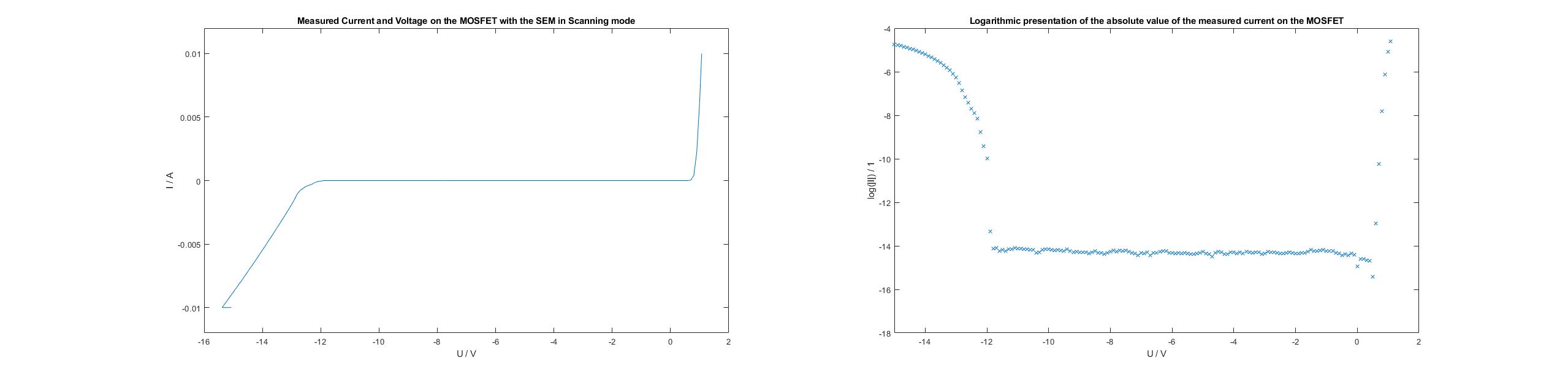
mA. This can be seen in figure 2. Afterwards the measurement was repeated
with the scanning mode of the
SEM turned on, providing an electron beam with an acceleration
current of 30 kV directed at the MOSFET. Figure 3 shows the results of
this measurement. In order to show potential small scale effects more clearly,
a logarithmic representation of the absolute values of the currents is
plotted as well.
Fig. 2: Output characteristics of a MOSFET Fig. 3: Output characteristics of a MOSFET while exposed
to a SEM scan.
Download: code.py
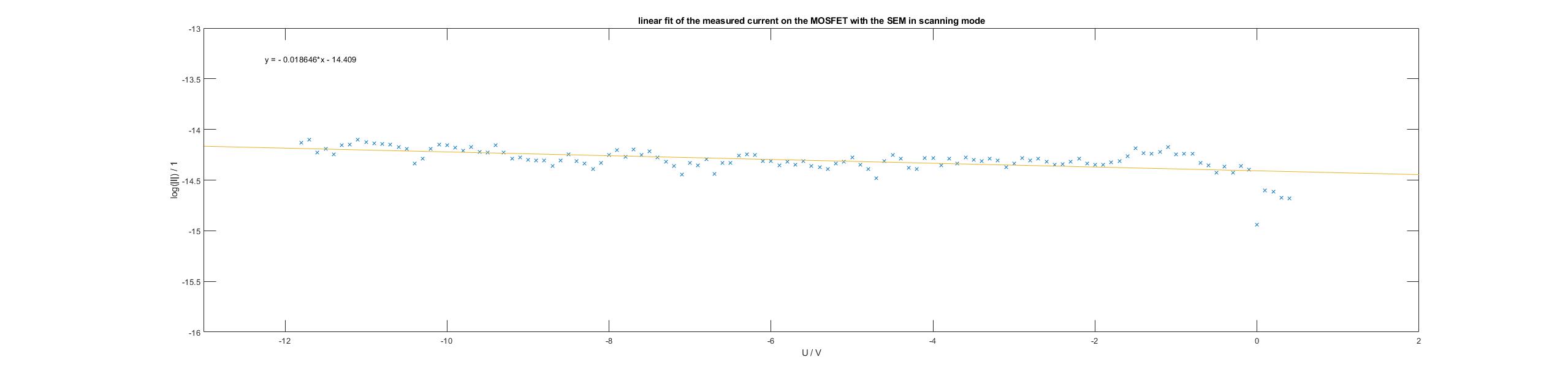
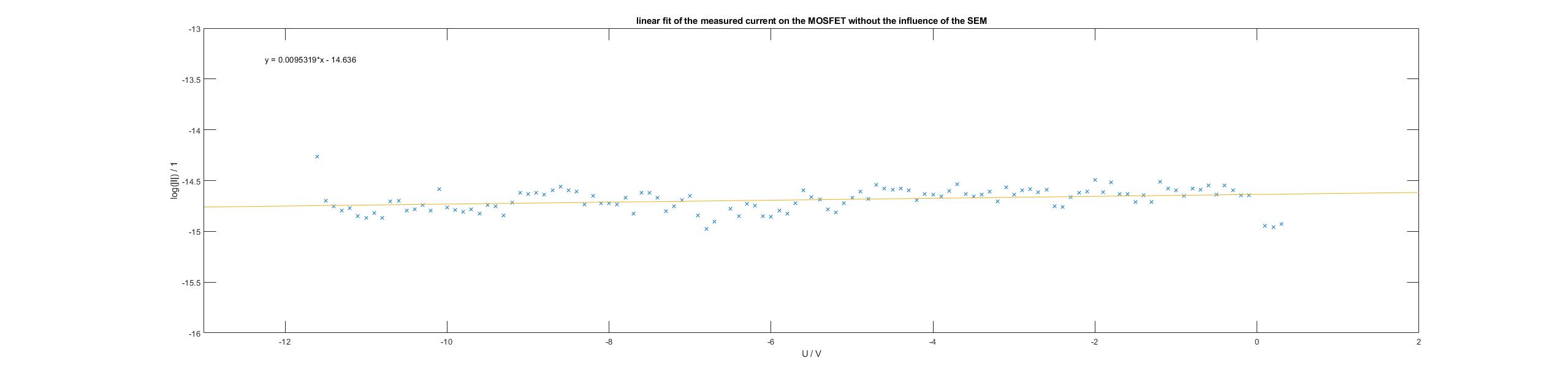
In the regions of near constant current in the reverse bias, linear fits of the currents
were created to show the offset between the two measurements more clearly.
These fits can be seen in figure 4 and 5. The figures show that the measured current
during the SEM scan is amplified. Fig. 4: Linear fit of the measurement during a SEM scan. Fig. 5: Linear fit of the measurement without influence from the SEM
This measurement indicades that the SEM's electron beam influences
the output characteristics of the MOSFET. The imaging
electrons are diverted to the Base and cause the current to be amplified.
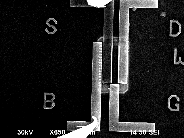
To further demonstrate this effect the SEM took two more pictures of the
MOSFET. In figure 6 the MOSFET is depicted without any voltage applied.
Figure 7 shows the MOSFET in reverse bias with -20 V applied. The blackening
of the source area shows that imaging electrons get diverted by the applied
voltage.
Fig. 6: MOSFET without applied voltage Fig. 7: MOSFET in reverse bias at -20 V
Measurement on a diode
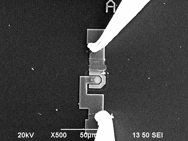
The diode on the surface of the chip that was used in the following experiment
is shown in figure 8.
Fig. 8: Diode with attached measuring pins.
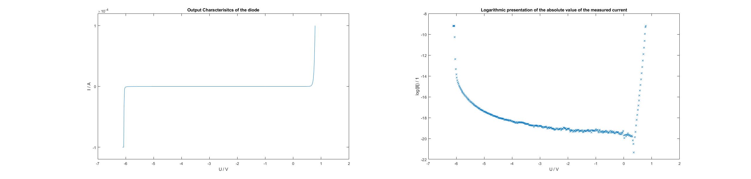
The two measuring pins were attached to the diode.
Two voltage sweeps were conducted with the current ranging
from -0.1 mA to 0.1 mA. Figure 9 shows the measured output characteristics
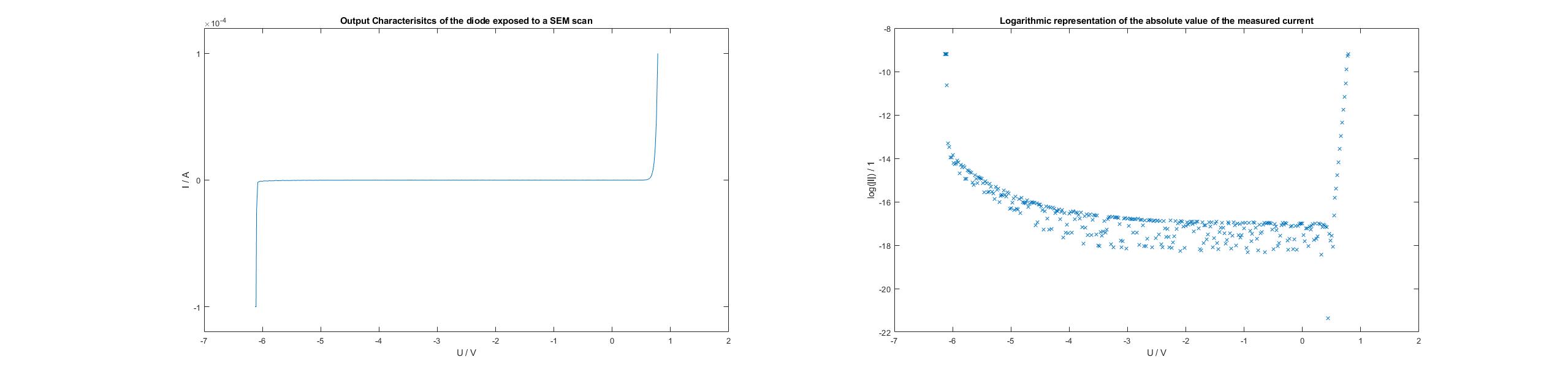
wit the SEM being turned off, figure 10 shows the same measurement
while the SEM is conducting a scan on the diode.
Fig. 9: Output characteristics of a diodeFig. 10: Output characteristics of a diode being exposed
to the electron beam of a SEM measurement
Download: code.py
The two figures demonstrate the influence of the electron beam on the output
characteristics of a diode. Similar to the measurement on the MOSFET, an
offset between the two measurements caused by the electron beam can be
observed, as an amplification of the current due to the imaging electron diverting.
As the currents in these experiments are sufficiently small, another
effect can be observed: On the logarithmic depiction of the current's absolute
value there seems to be a clear line as well as an area underneath with
lower currents. This may be caused due to the electron beams hitting the
probe with a certain frequency, as each beam only causes a measurement for a single
pixel on the output picture of the SEM. The beam's frequency could cause
higher currents on the diode output characteristics when it is activatedp0
and lower currents between the measurements of two pixels.
Conclusion
This experiment shows that the imaging beam of a SEM has a clear influence
on the output characteristics of diodes. This effect should be negligible
for currents much higher than the current induced by the beam. In order
to more precisely quantify this limit as well as effects caused by the beam's
sampling frequency, additional experiments should be conducted.