Saturation and transfer characteristics
Saturation characteristics
The output/saturation characteristics for different Gate-Source Voltages are shown in Figure 1.
The python code used to produce them is shown below.
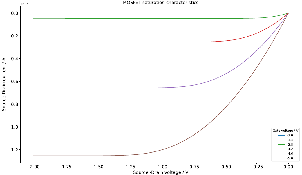 Source-Drain current plottet against the Source-Drain voltage for different Gate-voltages.
The output curves shown in Figure 1 should follow the output behavior as described by the gradual channal equations:
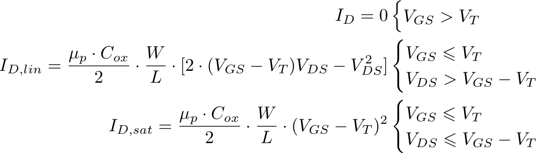
Figure 2: Formulas for the Output/Saturation Characteristics P-type MOSFET
The previous equations tell us about the three different operating regions of a MOSFET.
The first equation gives information about the cut-off region of an p-type MOSFET.
In this region no current is flowing trough.
The second equation describes the characteristics of a p-type MOSFET in the linear region.
The Drain Current ID in this zone depends on the dimensions (Width (W) and Length (L)) of the transistor,
the mobility μp, the specific capacitance of the gate Cox in F/m²,
the difference of the gate-source voltage VGS and the threshold voltage VT
but also on the drain-source voltage VDS.
The third equation gives information about the drain current ID in the saturation region.
The drain current dependents on the mobility μp, the specific capacitance of the gate Cox in F/m²,
the length L, the width W and the difference of the gate-source voltage VGS and the threshold voltage VT squared.
Transfer/Input characteristics
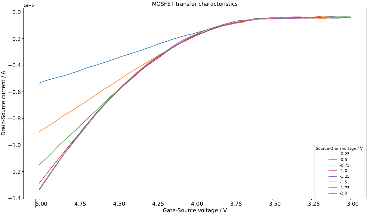 Drain-Source current plottet against the Gate-Source voltage for different Drain-voltages.
The Transfer/Input Characteristics define the change of the Drain-Source Voltage VDS with the change in the Drain Current ID
and the Gate-Source Voltage.
Drain-Source current plottet against the Gate-Source voltage for different Drain-voltages.
The Transfer/Input Characteristics define the change of the Drain-Source Voltage VDS with the change in the Drain Current ID
and the Gate-Source Voltage.