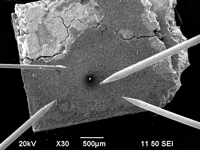
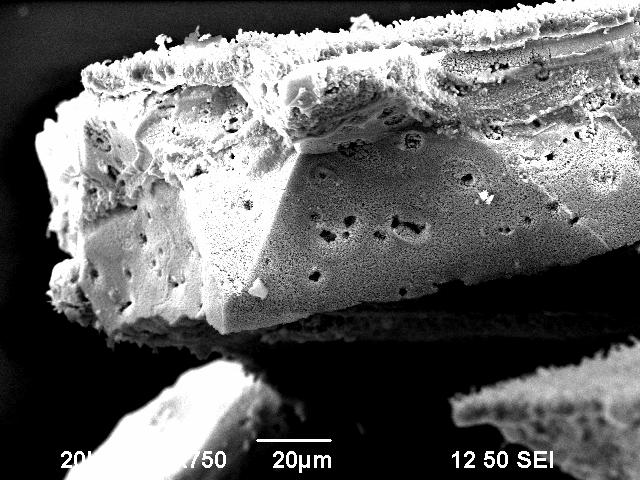
The porouse copper probe that was used in this experiment, previously broke into two halves. This accident however, led to some interesting results.
To get a more detailed overview over this topic, see
SEM-Wikipedia.
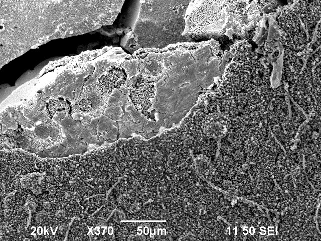
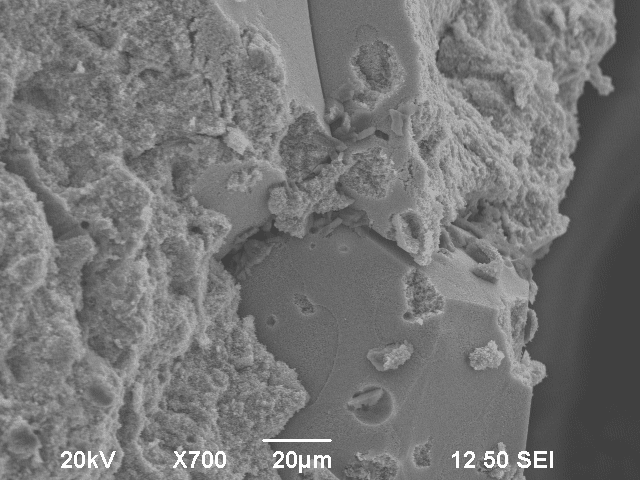
Using a scanning electron microscope, a more detailed observation of the surface could be made. Two different kinds of surfaces were visible using the equipment’s focused electron beam. On the one hand, there were small round structures, but on the other hand a very smooth surface was visible.
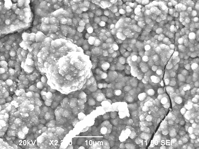
The bubble-like surface is due to oxidation of the copper probe. The scanning electron microscope has four very sharp tungsten carbide tips. These are used to hold certain probes down. Furthermore, they are electrically conducting and show a very low ohmic resistance of 4 $\Omega$ and therefore, they can be used to make 2-point and 4-point resistance measurements.
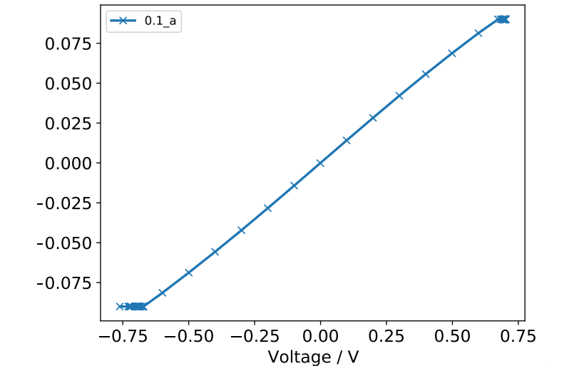
The tungsten carbide needle itself forms a thin oxide layer which leads to bad conductivity of the tip. To get rid of this oxide layer, scratching the needle onto the surface was not sufficient. Increasing the voltage between the two tips when connecting them together, however revealed a significant drop in resistance. Therefore, it was suspected that the oxide layer gets destroyed after a certain current is reached and as a consequence, of that, a temperature was reached, which destroyed this thin oxide layer.
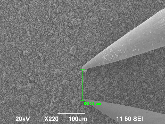
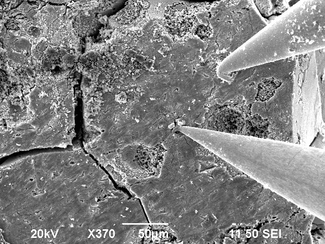
With two of these needles the following experiments were executed. The sharp tips are easily bent. It is important not to destroy them while trying to make contact with the surface. At first, we zoom onto the surface and focus on it. By modifying the brightness, contrast and focus parameters the quality of the picture can be improved. By changing the mode from Scan2 to Scan3 or Scan4, a much more detailed picture will be made over a longer period. Pressing freeze afterwards shows a clear, detailed and non-changing picture that can be saved.
Increasing the voltage also increases the electric field between the tips. This field hinders electrons from reaching the detector of the scanning electron microscope.
An insulating layer appears bright under the SEM since the electrons can’t move away and get easily excited by the electron beam. If the tips make contact with the surface, the brightness suddenly changes and the whole area gets dark, since the electrons can now flow away.
In order to prevent the tips from damage, the surface has to be in focus, so that one can see if the tip hits the surface. Afterwards, the first of the two needles will be lowered slowly. Once it gets closer to being into focus, it also is close to making contact with the surface. Contact is made if the surface as a whole moves when moving the tip, the tips itself bends or if we see structural changes at the landing point of the tip.
The bubble-like surface appears to flicker intensely while looking onto it with the scanning electron microscope. This is typically a sign of an insulator. Now using these needles to make an electrical contact confirms this suspicion that this structure has an extremely high resistance in the range of 8 $G\Omega$.
The smooth surface however had a very low ohmic resistance. This structure appears at the breaking lines. In the scanning electron microscope, it appears to be brighter than the bubble-like surface.
In a first try the 2-point resistance measurement showed an ohmic resistance of 200 $\Omega$ for the smooth surface, which is still very high, because the material is porouse copper.
As discussed above: After increasing the voltage, the thin oxcide layer on the tip was destroyed and an even lower resistance of around 8 $\Omega$ was measured. So the main resistance part in the 200 $\Omega$ measurement was from the tips.
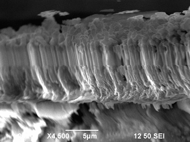
After a vertical observation of one of the fractures, it was visible that the bubble-like structure was in fact multiple columns which look like bubbles on the surface.
This experiment showed that it can be important to take an accurate look on the surface before making 2-point or 4-point measurements. The deep insight on the strikingly different surface conductivity, which was obtained during the SEM measurements would not be achievable through a simple 2-point or 4-point measurement. In the simple 2-point or 4-point measurement, one would most probably only have obtained a very low surface conductivity because the smooth, well conducting surfaces are only very small and localized.