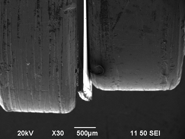
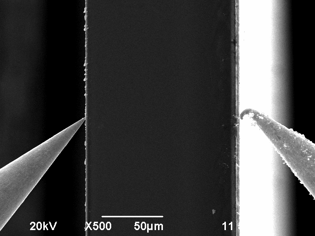
The next experiment also revolves around the scanning electron microscope. This time however, a broken wafer piece, which is kept in place by a copper sample holder, will be placed with its broken part upward into the SEM.
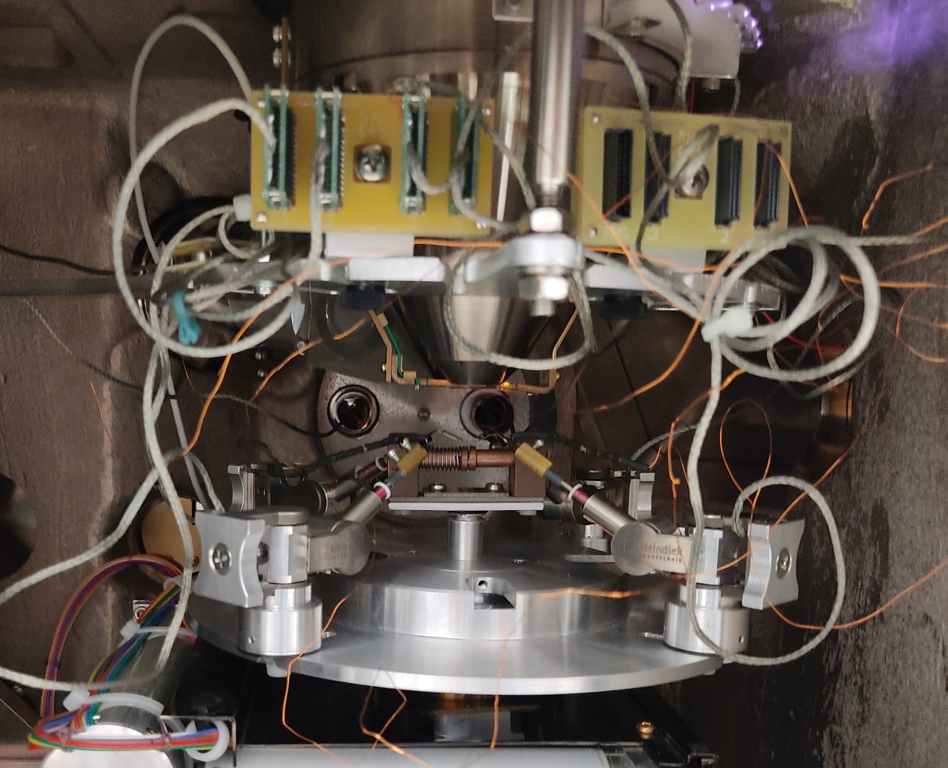
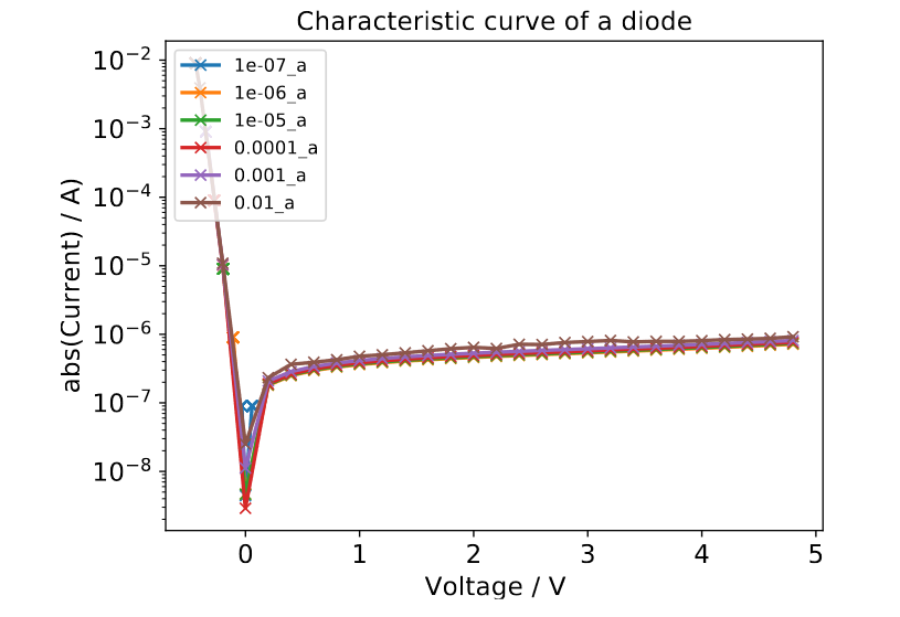
The tips were placed close to the sample, the lid was closed and the pumps activated. It is important to know the cables are correctly plugged in. Therefore, a quick measurement of the diode V-I curve was made beforehand to find forward and reverse direction of the diode. The measurements are performed with a sourcemeter unit (SMU). Keithley 2600 Series Sourcemeter. Afterwards, the Python program was used to make a measurement with different currents. It yielded the following result:
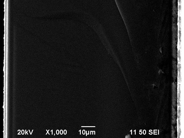
Some places may appear very bright, because they are steep (meaning there is a lot of surface area which can emit secondary electrons). Here the focused electron beam is able to generate a lot of secondary electrons. The measured wafer is around 120 $\mu$m thick. The following two pictures give a brief overview of the sample:
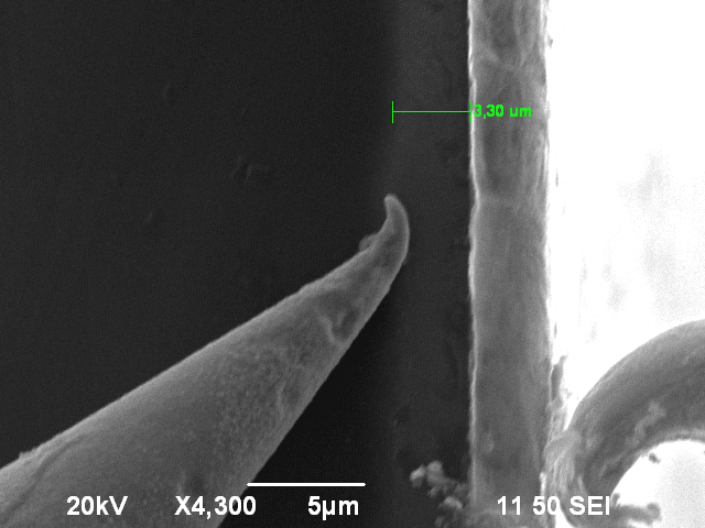
The transition between reverse bias voltage on and off made a white zone visible. However, at that time it was unclear what this zone was. A change in voltage appeared to shift the zone to the right. This however was just the deflection of the electron beam due to the higher voltage ⇒ the whole picture got shifted to the right ⇒ it is important to make position measurements with respect to some well distinctive layer of the material because then this overall shift of the picture makes no difference.
Since this zone is bright, and the rest of the wafer got dark, there is the theory that this should be the p-doped part of the diode + the depletion zone. This can be derived from the fact that we know that the diode is in reverse bias and hence the negative pole of the voltage source is connected to the p-doped side (when a voltage is applied on the sample, regions with more negative voltage are brighter because it is easier to remove electrons there). Below there is given a table, where the width $d$ of this bright zone was measured with respect to the reverse voltage $V_{reverse}$:
| $V_{reverse}$ / V | $d$ / $\mu$m |
|---|---|
| 5 | 3.38 |
| 10 | 3.42 |
| 20 | 3.69 |
| 40 | 3.91 |
| 70 | 4.13 |
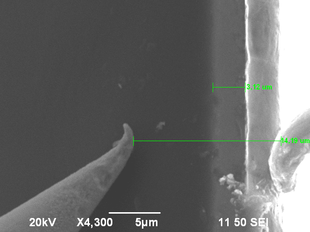
In order to verify this theory, an additional measurement was made where a reverse bias voltage is applied across the diode and the voltage on the wafer is measured by two SEM tips. There should be a more or less constant voltage drop in the non-depleted p-doped and n-doped areas, while there should be a fast change in the voltage drop across the depletion zone since the depletion zone has a much higher resistivity compared to the doped undepleted regions. This allows us to approximately localize the depletion zone. Since the tips are quite extended, the spatial accuracy of this method is very limited. However, by sweeping one of the probe tips over the surface it was possible to approximately find the depletion zone because it was possible to find the position where the voltage drop sharply changes. Below there is given a table with the results of that measurement. The distance $d$ is measured between the tip and the Aluminium layer on the right side and $V_{drop}$ is the voltage drop between the two attached SEM tips (one on the wafer and one applied to the Aluminium layer on the right).
| $d$ / $\mu$m | $V_{drop}$ / V |
|---|---|
| 41 | 4.8 |
| 4.0 | 4.3 |
| 3.3 | 1.4 |
| 1.2 | 0.04 |
This measured data gives the result that most of the depletion zone is located between 4 $\mu$m and 3.3 $\mu$m away from the left side of the Aluminium layer.
Starting position of the measurement:
Increasing the reverse voltage resulted in a widening of the bright zone, which would coincide with a growing depletion zone as explained in the following sentences. This width of the wide zone is hard to measure because the zone starts to smear out (the smeared out white part should be the depletion zone). In the following, there will be given an explanation about the smearing out of the white zone. At low bias voltages, one sees more or less a step function of the voltage across the depletion zone because it is difficult to get a meaningful contrast for small rest voltages like 0.5 V and additionally, the depletion zone is very small for small voltages. However, if the reverse bias voltage is increased, it becomes easier to see approximately the whole depletion zone bright because the rest voltage drop is still significant enough to give a good contrast in the SEM. Therefore, one sees this bright smeared out area because the depletion zone gets larger and larger with the voltage. So in this sense, it makes sense that for our measurements the width of the bright zone extends with increasing voltage because the bright zone is the undepleted p-doped area (very bright) + depletion zone (left part of bright zone + smeared out bright zone.
In the next two pictures we can see a slight increase of the bright region (p-doped layer + depletion zone).
Bright zone at a reverse bias voltage of 10 V.
Bright zone at a reverse bias voltage of 10 V.
In order to check the position of the depletion zone in a more accurate manner, another method was suggested, which uses a focused electron beam. When the electron beam hits the surface, it creates electron-hole pairs in the material. If this is done inside the depletion zone, the holes and electrons can be separated via the built-in electric field. The idea now is to connect the p-doped and n-doped area electrically via a current measuring unit (there was used: Stanford research systems SR570 - low noise current amplifier). This adds a path where the separated electrons and holes can move and so the current gives us a measure for the number of separated electron-hole pairs. The depletion zone is very successful at separating electron-hole pairs and hence, there is obtained a big current when the electron beam is focused on the depletion zone. If the beam is applied on a metal or doped undepleted material, most of the separated electrons and holes recombine again and give no additional current. Therefore, the measured current is mainly the beam current.
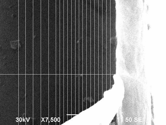
This method gives the opportunity to map the depletion zone of the diode. In order to do that, the electron beam is incrementally moved across the area where the depletion zone is expected. Below there is given a figure with the points where the electron beam was placed.
This gives the following map for the current depending on the distance from the left side of the Aluminium layer.

Overlapping this graph with the picture of the measurement pattern above yields:
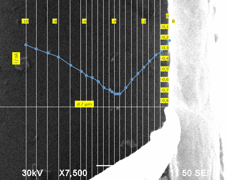
From this diagram, it is possible to state that the center of the depletion zone is around 3.6 $\mu m$ from the left side of the Aluminium layer which coincides well with the results from the previous measurement with the two SEM tips.
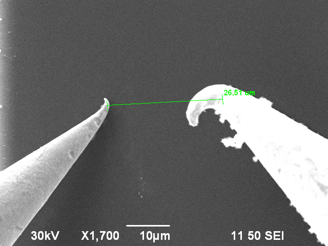
In a next step, the aim was to measure the conductivity of the n-substrate on the left side. As a first check, there was a 2-point resistance measurement with the tips positioned as in the picture below. This resulted in a resistance of 10.8 M$\Omega$. To calculate the resistivity the contact area must be known. Due to the deformation of the tips, no statement can be given about the dimensions of the contact area.
The 4-point method evades that drawback. If the probe is a thin film (thickness must be comparable small to the length and width) the resistivity of the material $\varrho$ is given by
\[ \begin{equation} \varrho = \frac{\pi wtV}{ln(2)l \cdot I} \end{equation} \]$V$ and $I$ are the voltage and current driven through the two outer needles and $l$, $w$ and $t$ are the length, width and thickness of the probe.
With the mobility $\mu_e$ and the charge $e$ of the electrons, the density of free electrons $n$ can be calculated. This density corresponds to the doping concentration of the semiconductor because the number of charge carriers generated from other sources is negligible at room temperature.
\[ \begin{equation} n = \frac{1}{e\mu_e \varrho} \end{equation} \]The doping concentration is too low to affect the mobility. Therefore the mobility of intrinsic silicon can be used, which is $1400 cm^2V^{-1}s^{-1}$. The measured device is a power diode where the p-doped region is in the $\mu$m range. It’s not possible to place all 4 tips on the p-doped region because it is too thin. As a consequence the resistance can’t be measured directly. With the depletion width, the charge carrier concentration of the p-doped region can be calculated
\[ \begin{equation} W = \sqrt{\frac{2\epsilon(N_A + N_D)V_{bi}}{eN_DN_A}} \end{equation} \]where $W$ is the width of the depletion zone, $N_A$ the concentration of acceptors, $N_D$ the concentration of donors, $\epsilon$ is the permittivity and $V_{bi}$ the built-in voltage of the diode. The concentration of acceptors is equal to the concentration of holes in the p-doped region and the concentration of donors is equal to the concentration of free electrons in the n-doped region. The permittivity can be approximated with the permittivity of Silicon. The built-in potential can be determined by operating the pn-junction in forward-bias. The concentration of holes $p$ can be expressed with
\[ \begin{equation} p = \frac{2\epsilon nV_{bi}}{W^2e n -2\epsilon V_{bi}} \end{equation} \]Here, we gave just a theoretical sketch how the doping concentrations could be calculated from the depletion width because due to technical issues, it was not possible to perform the necessary 4-point resistance measurement on the n-doped region.