|
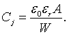
The capacitance of a pn junction depends on the width W of the depletion layer.
If the junction is heavily p-doped then it will be an asymmetric p+n junction where Na >> Nd. In this case the total depletion width is approximately equal to the depletion width on just the n-side of the junction.
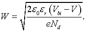
To experimentally characterize a pn-junction, often the capacitance is measured as a function of the applied voltage. For an abrupt p+n junction, a plot of 1/Cj² versus V is a straight line. The formula can be determined from the above two equations. The slope and intercept of this line give the doping concentration and built-in potential.
The capacitance-voltage characteristic of a silicon p+n-junction with an area of 0.004 cm² is measured. The results of this measurement are shown in the table on the right.
What is the doping concentration and the built-in potential?
The dielectric constant of silicon is εr = 11.9.
|