Problem 1
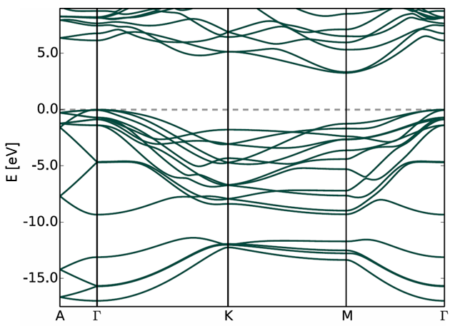
4H-SiC is a semiconductor with a bandgap of 3.3 eV. The band diagram is shown below.

(a) Could you use 4H-SiC to build a light emitting diode? What color light would it emit? Explain your reasoning.
(b) How many effective masses would be needed to describe the holes at the top of the valence band? How many effective masses would be needed to describe the electrons at the bottom of the conduction band band? Explain your reasoning.
(c) The effective density of states in the conduction band at 300 K is $1.7 \times 10^{19}\quad\text{cm}^{-3}$ and the effective density of states in the valence band at 300 K is $2.5 \times 10^{19}\quad\text{cm}^{-3}$. What is the concentration of holes in intrinsic 4H-SiC at 300 K?
Solution
Problem 2
Consider a Schottky diode (metal - $n$-semiconductor) and a $p^+n$ diode where the $p^+$ region is doped so heavily that the semiconductor is degenerate. Since the Fermi energy of a degenerately doped $p^+$ semiconductor is in the valence band, it behaves like a metal.
(a) Draw the band diagrams for these two diodes (conduction band, valence band, Fermi energy).
(b) Why is the current in a forward biased Schottky diode dominated by thermionic emission while the current in a forward biased $p^+n$ diode is dominated by diffusion?
(c) Why does the Schottky diode respond faster than the $p^+n$ diode?
Problem 3
(a) Draw an $p$-channel MOSFET showing the source, drain, gate, and body contacts.
(b) Draw the band diagram (conduction band, valence band, Fermi energy), and the electric field as a function of position in a MOS capacitor with a $n$-type substrate in inversion.
(c) Consider a MOSFET in the linear regime (the gate is above the threshold to induce an inversion layer in the channel but the drain voltage is not so high as to cause pinch-off). How does the depletion width vary along the channel from source to drain?
(d) Explain what latch-up is in CMOS circuits.
Problem 4
A $pnp$ bipolar transistor is constructed from GaAs, a direct bandgap semiconductor.
(a) What would be the advantages and disadvantages of using GaAs instead of silicon to make a bipolar transistor?
(b) When the emitter-base junction is forward biased, is light emitted like in a light emitting diode? Explain your reasoning.
(c) Draw the minority carrier concentration in a pnp transistor in biased in the forward active regime.
(d) How can you calculate the collector current?