Problem 1
An intrinsic silicon sample is doped with acceptors from one side such that $N_A=N_0\exp (-ax)$.(a) Draw the band diagram (conduction band, valence band, Fermi energy) as a function of $x$. There is no current flowing so the Fermi energy should be constant.
(b) Draw the electron and hole concentrations ($n$ and $p$) and the electric field as a function of $x$. Explain why these quantities have the form you have drawn.
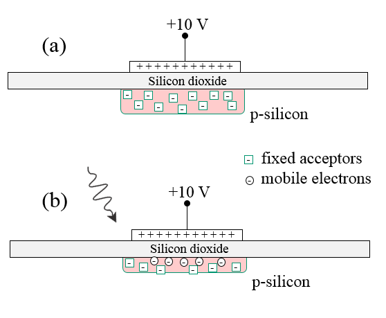
Problem 2 CCD cameras us MOS capacitors to trap mobile charge. First a positive voltage is applied to the gate of a MOS capacitor. This depletes the region under the gate as in figure (a).

(a) Draw the band diagram (conduction band, valence band, Fermi energy) along a line going from the metal across the oxide into the semiconductor. The p-type semiconductor is in depletion.
(b) Draw the electric field and the charge density. Mark the position of acceptor concentration $N_A$ on the charge density axis.
(c) Light falls on this device and mobile electrons are collected at the silicon/oxide interface as in figure (b). Draw the electric field and the charge density for this situation. The positive and negative charges should balance on the the MOS capacitor before and after light strikes it. What is the consequence of the charge neutrality for the electric field at the semiconductor/oxide interface?
Problem 3
(a) Draw a pnp bipolar transistor showing the emitter, collector, and base contacts.
(b) What are the doping levels of the emitter, the base, and the collector? How does the doping affect the emitter efficiency and the base transport factor?
(c) Explain how the collector current is calculated.
(d) Why would a bipolar transistor be used in a common base configuration?
Problem 4
Infrared light emitting diodes are used in remote controls.
(a) Draw the electron dispersion relation $E$ vs. $k$. Indicate the value of the bandgap $E_g$.
(b) Draw a cross section of a wafer with an LED. Include the contacts in the drawing.
(c) Explain what total internal reflection is and why in reduces the efficiency of an LED.
(d) What is the longest wavelength that can be produced with an infrared LED?
Quantity | Symbol | Value | Units | |
| electron charge | e | 1.60217733 × 10⁻¹⁹ | C | |
| speed of light | c | 2.99792458 × 10⁸ | m/s | |
| Planck's constant | h | 6.6260755 × 10⁻³⁴ | J s | |
| reduced Planck's constant | $\hbar$ | 1.05457266 × 10⁻³⁴ | J s | |
| Boltzmann's constant | kB | 1.380658 × 10⁻²³ | J/K | |
| electron mass | me | 9.1093897 × 10⁻³¹ | kg | |
| Stefan-Boltzmann constant | σ | 5.67051 × 10⁻⁸ | W m-2 K-4 | |
| Bohr radius | a0 | 0.529177249 × 10⁻¹⁰ | m | |
| atomic mass constant | mu | 1.6605402 × 10⁻²⁷ | kg | |
| permeability of vacuum | μ0 | 4π × 10-7 | N A-2 | |
| permittivity of vacuum | ε0 | 8.854187817 × 10⁻¹² | F m-1 | |
| Avogado's constant | NA | 6.0221367 × 10²³ | mol-1 |