PHT.301 Physics of Semiconductor Devices
|
|
PHT.301 Physics of Semiconductor Devices | |
|
|
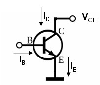
Common emitter configurationIn a common emitter configuration the base current controls the collector current.
The Ebers-Moll model for a bipolar transistor is, $ I_E=I_{ES}\left[\exp\left(\frac{eV_{BE}}{k_BT}\right)-1\right]-\alpha_R I_{CS}\left[\exp\left(\frac{eV_{BC}}{k_BT}\right)-1\right],$ $ I_C=\alpha_F I_{ES}\left[\exp\left(\frac{eV_{BE}}{k_BT}\right)-1\right]- I_{CS}\left[\exp\left(\frac{eV_{BC}}{k_BT}\right)-1\right],$ $I_B=I_E-I_C.$ The saturation currents are, \[ \begin{equation} I_{ES} = Aen_i^2\left(\frac{D_{pe}}{(x_e-d_e)N_{de}} + \frac{D_{nb}}{(x_{bc}-d_{eb})N_{ab}}\right)\qquad I_{CS} = Aen_i^2\left(\frac{D_{pc}}{(d_c-x_c)N_{dc}} + \frac{D_{nb}}{(x_{bc}-x_{eb})N_{ab}}\right), \end{equation} \]and \[ \begin{equation} \alpha_RI_{CS} =\alpha_FI_{ES} = Aen_i^2\left(\frac{D_{nb}}{(x_{bc}-x_{eb})N_{ab}}\right). \end{equation} \]Here $A$ is the area of the pn-junctions, $e$ is the elementary charge, $N_{de}$ is the donor concentration of the emitter, $N_{ab}$ is the acceptor concentration of the base, $N_{dc}$ is the donor concentration of the collector, $x_e-d_e$ is the distance from the metal contact of the emitter to the edge of the depletion with in the emitter, $x_{bc}-x_{eb}$ is the neutral base width (between the depletion widths in the base), $d_c-x_c$ is the distance from the metal contact of the colector to the edge of the depletion with in the collector, $D_{pe}$ is the diffusion constant of minority holes in the emitter, $D_{nb}$ is the diffusion constant of minority electrons in the base, and $D_{pc}$ is the diffusion constant of minority holes in the collector. The diffusion constants of the electrons and holes are related to the mobilities by the Einstein relation, \[ \begin{equation} D_n=\frac{\mu_nk_BT}{e}\hspace{1.5cm}D_p=\frac{\mu_pk_BT}{e}, \end{equation} \]where $\mu_n$ is the mobility of the electrons and $\mu_p$ is the mobility of the holes. The intrinsic carrier concentration is, \begin{equation} n_i=\sqrt{N_c\left(\frac{T}{300}\right)^{3/2}N_v\left(\frac{T}{300}\right)^{3/2}}\exp\left(\frac{-E_g}{2k_BT}\right), \end{equation}where $N_c$ is the effective density of states in the conduction band at 300 K, $N_v$ is the effective density of states in the valence band at 300 K, and $E_g$ is the band gap. The following Once $I_{ES},\,I_{CS},\,\alpha_F$ and $\alpha_R$ are known, the Ebers-Moll model can be solved to plot the collector current $I_C$ as a function of $V_{CE}$ for different base currents $I_{B}$. The Ebers-Moll equations used here do not include the Early effect or breakdown at large $V_{CE}$. Below $I_C$ is plotted against $V_{CE}$ for the values of $I_B$ in the table on the right.
|