PHT.301 Physics of Semiconductor Devices
|
|
PHT.301 Physics of Semiconductor Devices | |
|
|
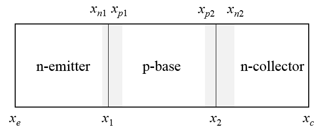
Minority carrier concentration of an npn bipolar transistorThe currents flowing through a bipolar transistor can be calculated from the minority carrier concentrations in the emitter, the base, and the collector. If no voltages are applied across the two pn-junctions of the transistor, then the minority carrier concentrations are constant. Diffusion currents are proportional to the gradient of the minority carrier concentration so when there are no voltages applied across the junction, no current flows. If voltages are applied, there will be concentration gradients in the the emitter, the base, and the collector which can be determined by solving the diffusion equation in each of these three regions. Consider an npn bipolar transistor. Let \(x_e\) be the position of the metal-semiconductor contact of the emitter, \(x_1\) be the position of the emitter-base pn junction, \(x_2\) be the position of the base-collector pn junction, and \(x_c\) be the position of the metal-semiconductor contact of the collector.
The gray areas in the drawing represent the depletion region around the pn-junctions. Let \(x_{n1}\) be the position of the edge of the depletion width of junction 1 on the n-side and \(x_{p1}\) be the position of the edge of the depletion width of junction 1 on the p-side. Similar definitions are made for junction 2. The depletion widths \(W_1\) and \(W_2\) depend on the voltages \(V_1\) and \(V_2\) across the two pn-junctions. The emitter-base depletion width is, $$W_1 = \sqrt{\frac{2\epsilon (N_{de}+N_{ab})(V_{bi1}-V_1)}{eN_{de}N_{ab}}},$$and the base-collector depletion width is, $$W_2 = \sqrt{\frac{2\epsilon (N_{dc}+N_{ab})(V_{bi2}-V_2)}{eN_{dc}N_{ab}}},$$ where \(\epsilon\) is the permittivity constant of the semiconductor, \(N_{de}\) is the concentration of donors in the emitter, \(N_{ab}\) is the concentration of acceptors in the base, \(N_{dc}\) is the concentration of donors in the collector, \(e\) is the elementary charge, and the voltges \(V_1\) and \(V_2\) are taken to be positive if the junction is forward biased. The built-in voltages of the two junctions are, $$V_{bi1}=\frac{k_BT}{e}\ln\left(\frac{N_{de}N_{ab}}{n_i^2}\right),\qquad V_{bi2}=\frac{k_BT}{e}\ln\left(\frac{N_{dc}N_{ab}}{n_i^2}\right).$$Here \(k_B\) is Boltzmann's constant, \(T\) is the absolute temperature, and \(n_i\) is the intrinsic carrier concentration, \(n_i=\sqrt{N_cN_v}\left(\frac{T}{300}\right)^{3/2}\exp\left(\frac{-E_g}{2k_BT}\right)\), where \(N_c\) is the effective density of states in the conduction band at 300 K, \(N_v\) is the effective density of states in the valence band at 300 K, and \(E_g\) is the band gap of the semiconductor. The positions of the edges of the depletion regions are, $$x_{n1} = x_1-\frac{N_{ab}W_1}{N_{ab}+N_{de}},\qquad x_{p1} = x_1+\frac{N_{de}W_1}{N_{ab}+N_{de}}, \qquad x_{n2} = x_2+\frac{N_{ab}W_2}{N_{ab}+N_{dc}},\qquad x_{p2} = x_2-\frac{N_{dc}W_2}{N_{ab}+N_{dc}}.$$Let the concentration of minority holes in the emitter be \(p_e(x)\). The hole concentrations at the edges of the neutral region of the emitter are, $$p_e(x_e)=p_{e0}=\frac{n_i^2}{N_{de}},\qquad p_e(x_{n1})=N_{ab}\exp\left(\frac{-e(V_{bi1}-V_1)}{k_BT}\right)=p_{e0}\exp\left(\frac{eV_1}{k_BT}\right).$$Here \(p_{e0}\) is the equilibrium concentration of holes in the emitter. Similarly, the concentrations of minority electrons in the base \(n_b(x)\) and minority holes in the collector \(p_c(x)\) at the edges of the neutral regions of the base and the collector are, $$n_b(x_{p1})=N_{de}\exp\left(\frac{-e(V_{bi1}-V_1)}{k_BT}\right)=n_{b0}\exp\left(\frac{eV_1}{k_BT}\right),\qquad n_b(x_{p2})=N_{dc}\exp\left(\frac{-e(V_{bi2}-V_2)}{k_BT}\right)=n_{b0}\exp\left(\frac{eV_2}{k_BT}\right),$$ $$p_c(x_{n2})=N_{ab}\exp\left(\frac{-e(V_{bi2}-V_2)}{k_BT}\right)=p_{c0}\exp\left(\frac{eV_2}{k_BT}\right),\qquad p_c(x_c)=p_{c0}=\frac{n_i^2}{N_{dc}},$$where \(n_{b0}\) is the equilibrium concentration of electrons in the base and \(p_{c0}\) is the equilibrium concentration of holes in the collector. The minority carrier concentrations can be found by solving the diffusion equation in the emitter, and base, and the collector. The diffusion equation in the emitter is, $$D_{pe}\frac{d^2p_e}{dx^2}=\frac{p_e-p_{e0}}{\tau_{pe}},$$where \(D_{pe}\) is the diffusion constant for holes in the emitter, and \(\tau_{pe}\) is the minority carrier lifetime for holes in the emitter. The diffusion constant is related to the carrier mobility by the Einstein relation \(D = \mu k_BT/e\), where \(\mu\) is the charge carrier mobility. The solution to the diffusion equation for the minority hole concentration in the emitter has the form, $$p_e(x)=A_e\exp (x/L_{pe})+B_e\exp (-x/L_{pe}),$$where \(L_{pe}=\sqrt{D_{pe}\tau_{pe}}\) is the diffusion length for minority holes in the emitter and the boundary conditions can be used to determine \(A_e\) and \(B_e\), $$A_e=\frac{p_e(x_e)\exp (x_e/L_{pe})-p_e(x_{1n})\exp (x_{1n}/L_{pe})}{\exp (2x_e/L_{pe})-\exp (2x_{1n}/L_{pe})},$$ $$B_e=\frac{p_e(x_e)\exp (-x_e/L_{pe})-p_e(x_{1n})\exp (-x_{1n}/L_{pe})}{\exp (-2x_e/L_{pe})-\exp (-2x_{1n}/L_{pe})}.$$Similar derivations can be made for the minority electron concentration in the base and the minority hole concentration in the collector. $$n_b(x)=A_b\exp (x/L_{nb})+B_b\exp (-x/L_{nb}),\qquad\qquad p_c(x)=A_c\exp (x/L_{pc})+B_c\exp (-x/L_{pc}),$$ $$A_b=\frac{n_b(x_{p1})\exp (x_{p1}/(L_{nb})-n_b(x_{p2})\exp (x_{p2}/(L_{nb})}{\exp (2x_{p1}/(L_{nb})-\exp (2x_{p2}/(L_{nb})},\qquad\qquad A_c=\frac{p_c(x_{n2})\exp (x_{n2}/L_{pc})-p_c(x_c)\exp (x_c/L_{pc})}{\exp (2x_{n2}/L_{pc})-\exp (2x_c/L_{pc})}$$ $$B_b=\frac{n_b(x_{p1})\exp (-x_{p1}/(L_{nb})-n_b(x_{p2})\exp (-x_{p2}/(L_{nb})}{\exp (-2x_{p1}/(L_{nb})-\exp (-2x_{p2}/(L_{nb})},\qquad\qquad B_c=\frac{p_c(x_{n2})\exp (-x_{n2}/L_{pc})-p_e(x_c)\exp (-x_c/L_{pc})}{\exp (-2x_{n2}/L_{pc})-\exp (-2x_c/L_{pc})}.$$The derivatives of the minority carrier concentrations are, $$\frac{dp_e(x)}{dx}=\frac{A_e}{L_{pe}}\exp (x/L_{pe})-\frac{B_e}{L_{pe}}\exp (-x/L_{pe}),$$ $$\frac{dn_b(x)}{dx}=\frac{A_b}{L_{nb}}\exp (x/L_{nb})-\frac{B_b}{L_{nb}}\exp (-x/L_{nb}),$$ $$\frac{dp_c(x)}{dx}=\frac{A_c}{L_{pc}}\exp (x/L_{pc})-\frac{B_c}{L_{pc}}\exp (-x/L_{pc}).$$The electron current flowing through the emitter-base junction \(I_{en}\) and the hole current flowing through the emitter-base junction \(I_{ep}\) are, $$I_{en}=-A_{eb}eD_{nb}\frac{dn_b(x_{p1})}{dx},\qquad I_{ep}A_{eb}eD_{pe}\frac{dn_b(x_{n1})}{dx},$$where \(A_{eb}\) is the area of the emitter-base junction. The total emitter current is \(I_{en}+I_{ep}\). The electron current flowing through the base-collector junction \(I_{cn}\) and the hole current flowing through the emitter-base junction \(I_{cp}\) are, $$I_{cn}=-A_{eb}eD_{nb}\frac{dn_b(x_{p2})}{dx},\qquad I_{cp}=A_{eb}eD_{pc}\frac{dp_c(x_{n2})}{dx}.$$The active area of the collector is the same as the area where the electrons are emitted \(A_{eb}\). The total collector current is \(I_{cn}+I_{cp}\). The base current is the emitter current minus the collector current \( I_b = I_e-I_c\). The collector-emitter voltage is \(V_{ce}=V_1-V_2\). The form below calculates the minority carrier distribution for an npn bipolar transistor. \(E_g=\) eV; \(n_i=\) cm-3; \(V_{bi1}=\) eV; \(V_{bi2}=\) eV; \(W_1=\) μm; \(W_2=\) μm;
|