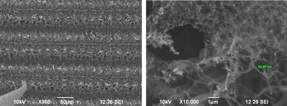
Laser Induced Graphene (LIG) is a material based on Carbon which is produced via a high intense laser beam. The carbon forms into nanotubes in the direction of the laser beam. With the intensity of the laser beam you can manipulate the porosity of the nanotubes. An SEM was used to analyze the structure of the material. To get more information about an SEM-Measurement you can look up the following link. The LIG is fixed on a plastic plate, therefor it is necessary to bring the material in contact with a metal tip inside the SEM, otherwise there would be a charging effect from the electron-beam. The left image of Figure 1 shows the nanotubes, the right image the structure of LIG.
Figure 1: Showing an overview of the nanotubes (left) and a closeup of the structure (right)
The current was measured through tips made of tungsten carbide for different voltages to get an idea of the conductivity. The Python script used is added below, as are the measured values. From that the conductivity and the conductivity per unit length (Table 1) was calculated. It can be seen that the current does change linearly with the distance between the tips, leading to the assumption that there are relatively high contact resistances at play.
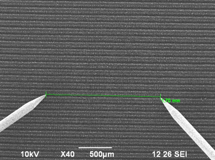
Figure 2: Showing the setup of the conductivity measurement between the two tips, which are in line with the LIG nanotube structure.
It was also checked whether the resistance in direction of the nanotubes is different to the resistance perpendicular to the nanotubes. However, no noticeable difference was recorded which could be due to a good conduction between the edges of the material or due to a better conducting layer of carbon underneath the nanotubes.
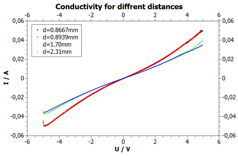
Figure 3: Conductivity measured inline with the nanotubes for different tip distances.
The following table shows the different resistances $R$ and resistivities $\rho$ measured for different distances $d$ inline and perpendicular to the nanotubes:
| Position | $d$ / cm | $R$ / [$\Omega$] | $\rho$ / [$\Omega$cm] |
| inline | 0.087 | 1.059 x 10$^{-4}$ | 9.18 x 10$^{-6}$ |
| inline | 0.089 | 1.062 x 10$^{-4}$ | 9.49 x 10$^{-6}$ |
| inline | 0.170 | 1.404 x 10$^{-4}$ | 2.39 x 10$^{-5}$ |
| inline | 0.231 | 1.466 x 10$^{-4}$ | 3.39 x 10$^{-5}$ |
| perpendicular | 0.145 | 1.355 x 10$^{-4}$ | 1.96 x 10$^{-5}$ |
To get more meaningful values for the conductivity it is necessary to neglect the resistance at the contacts. Therefor a four-point-current-voltage-measurement was used. More details on the four-point-measurement can be found here
The code to run a python program to measure the resistance is given below. The program repeats the measurement for 200 times to get meaningful results. In figure 5 one can see, that there is a large difference between the four-point measurement and the normal resistance measurement. A noticeable drop of resistance was recorded at the beginning of each measurement. This could be explained by a temperature change of the sample due to the measurements, however no further investigations were done at this point.
could not explain why the resistance is dropping at the beginning, but it was consistent. Maybe it was because of a temperature change of the sample, because of the measurements.

Figure 4: Comparison of the Resistance measured in the 2 wire and 4 wire setup
To measure the temperature dependence on the resistance of the LIG, the resistance R was measured at two degree intervals from 10 degrees to 40 degrees and also from 40 degrees to 10 degrees with a waiting time of 60 s to between measurements to temperate the sample. The first results of this measurement showed a hump for the first few temperature points, suggesting that the waiting time was too low, therefore the experiment was repeated with a waiting time of 10 minutes. Here the bump is still visible but not as pronounced, suggesting that it was indeed time the climate chamber needs to temperate that affected the results and if the waiting time was increased further, better results could be achieved. The results of the second measurements are seen in the two figures below. The Python Script is also added below
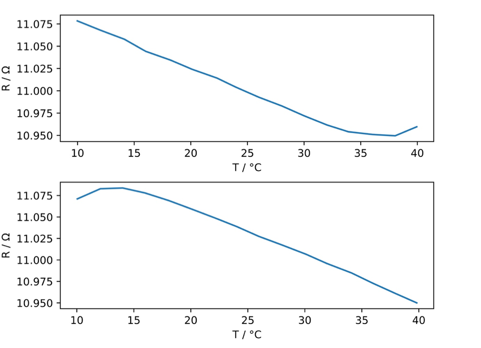
Figure 5: Showing the temperature dependence of the resistance R of the LIG sample with decreasing temperature T (top) and increasing temperature T (bottom).
The result of the temperature dependence, as it is shown, is that the resistivity falls with increasing temperature. It can also be seen that the linearity is quite similar in both cases, as is expected. This leads to the conclusion the sample acts like a non-metal. The temperature coefficient $\alpha$ was calculated by considering the temperature resistance curve as linear and the following formula could be used:
\begin{equation} R(T) = R(T_0)*(1+\alpha_{T_0}*(T-T_0)) \end{equation} \begin{equation} \alpha=\frac{R(T)-R(T_0)}{R(T_0)*(T-T_0)} \end{equation}For the calculation only values in the Temperature interval from 35-10 degrees and from 15-40 degrees were considered. This gave two calculated values for $\alpha_{T}$ where T denotes the initial temperature of the interval:
\begin{equation} \alpha_{\text(35)}= -0,42*10^{-3}\frac{\Omega}{K} \end{equation} \begin{equation} \alpha_{\text(15)}= -0,47*10^{-3}\frac{\Omega}{K} \end{equation}Comparing this to the literature value of carbon $\alpha_{C}=-0.5x10^{-3}$ K$^{-1}$ it shows that the results are comparable, however to give a better and more valuable comparison the experiment would need to be repeated and a longer waiting time would need to be set to accommodate for the time it takes for the climate chamber to temperate.
Electron Beam Induced Current (EBIC) is a technique which is used to identify junctions and measure currents that flow in a semiconductor. A sample is placed into a Scanning Electron Microscope (SEM) and the microscopes electron beam creates electron hole pairs in the sample and given an electric field a current can flow. The electron beam is scanned across the sample and the variations in the induced current are mapped and displayed in colour contrasted images.
EBIC measurements were used in order to determine whether LIG was an n-type or a p-type semiconductor. For this a LIG sample was placed into the SEM and measuring tips made of tungsten carbide were buried into the graphene to ensure good contact. The image below shows a simple schematic of the setup:
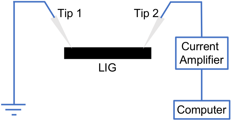
Figure 6: Image showing a simple schematic of the EBIC measurement setup. One of the measurement tips was grounded and one of the tips was connected to a current amplifier. These tips will be referred to as Tip 1 and Tip 2 respectively.
For the EBIC measurements the acceleration current of the SEM was set to 30 KV and a spot size of 90 was used. Figure 7 shows the first scans:
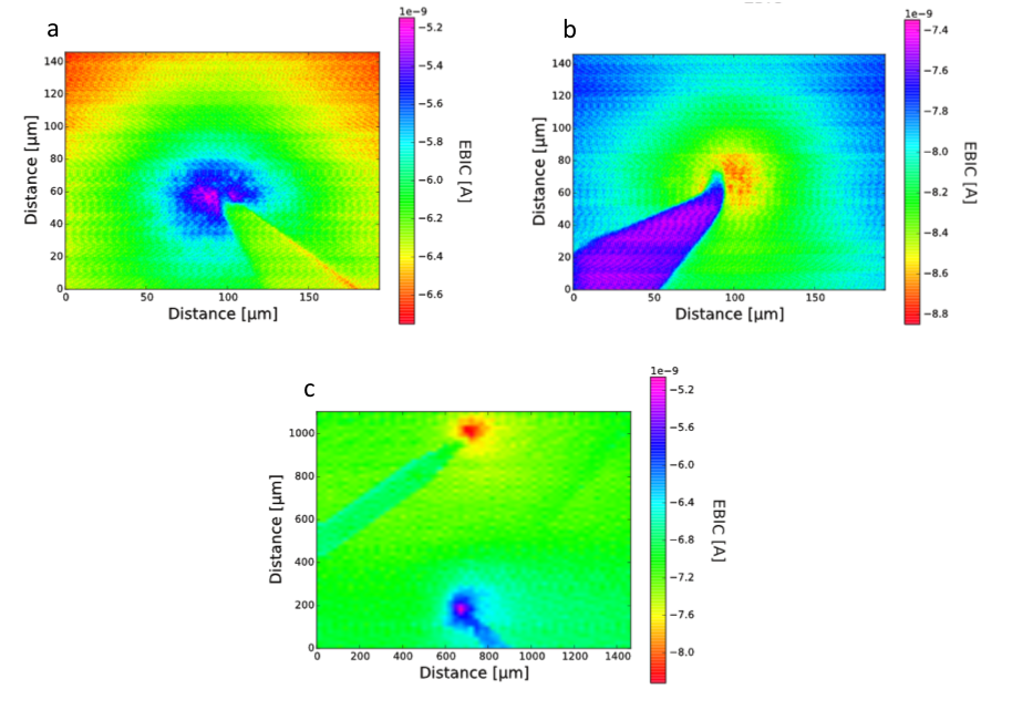
Figure 7: I Image showing the first EBIC measurement. Image a shows a scan around Tip 1, image b a scan around Tip 2 and image c a scan with Tip 1 at the bottom and Tip 2 at the top.
What should be noted first is that the measured current is always neagtive. This may be due to an offset which was attempted to be measured using a faraday cup however the measruemetns were inconlcusive so it was decided to ignore the offset. What can nonetheless be clearly seen is that the current around Tip 2 is more negative than the current around Tip 1. This suggests that there is a current flowing out of the current amplifier, meaning that there is an electric field pointing from the LIG into the tip. Given that the contact point is a shotky contact (metal-semiconductor contact) an electric field pointing into the tip i.e. from the semiconductor to the metal, suggests that the LIG is a
p-type semiconductor.
To further test this, the measurement was repeated, however a drop of silver paste was added to the LIG to ensure a better contact. The results are shown in figure 8:

Figure 8: Image a shows an SEM image of the LIG sample with Tip 2 buried in the Silver paste. Image b shows the EBIC measurement with Tip 1 at the bottom and Tip 2 at the top. It is evident that the entire region surrounding the silver paste shows a more negative current than the region surrounding Tip 1, further supporting the previous finding.
Another experiment to determine whether LIG is an n- or a p-type semiconductor is the Seebeck Effect For this a simple Multimeter was used where one of the inputs was connected to a hot tip of a soldering iron. The sign of the measured current would then give insight as to which type semiconductor the LIG is. At first the positive lead was connected to the soldering iron. Given a p-type semiconductor, where the mobile charge carriers are holes, a positive current was expected. However, the results were inconclusive. The current was positive at first, however it was extremely small to begin with and seemed to jump between positive and negative. It seemed to make no difference where on the sample the tips were placed. Even repeating the experiment with the negative lead connected to the soldering iron had little effect. This could be explained by the fact that the graphene layer is very thin and a decent conductor of heat, meaning that it is possible that the entire sample was heated quickly enough that the Seebeck Effect could not be discerned.