Measurement Setup
The measurement is done inside the scanning electron microscope (SEM). The SEM setup is used for the electron beam induced current (EBIC) measurement and to accurately place the probe needles onto the pads of the measured circuit. The electrical measurements are then done using the Keithley 2636 sourcemeter unit (SMU) connected to a measurement PC.
Insights Gained by SEM Imaging
The measured chip was firstly examined using the SEM to find any interesting features to measure. The measured device can be seen below. With some previous knowledge, this looks like a power MOSFET (LDMOS) with a Z-diode (ZDIO) connected to the gate-contact to protect the gate oxide from ESD damage.

Measured Device and Probe Connections
The measured devices are a power mosfet (LDMOS) and a Z-diode (ZDIO) that protects the gate. SMU A is connected to the gate contact, while SMU B is connected to the transistor's drain.Electrical Measurements and Results
To allow a full electrical characterization of the MOSFET, both channels of the SMU were used. Channel A controls the gate contact (SMU A HI) while channel B (SMU B HI) is connected to measure drain current and voltage. Both channels share the same reference node (SMU A/B LO) at the combined source/bulk connection.
Gate Protection Diode
The gate protection diode (ZDIO) is measured first. This measurement gives a valid range for the gate voltage and hints to whether we measure an N-channel or an P-channel device. The code for the measurement is listed below.
It produces the following results. From this we can conclude that the Z-diode clamps the gate voltage to about 20 V. Z-diodes are normally operated in reverse bias, thus it conducts for voltages below 0 V. From this, we conclude that the gate voltage is higher than the source in operation and the transistor must be of N-channel type. The measurement of the body diode and the EBIC measurement will confirm this expectation.

Gate Protection Diode Measurement [gate_leakage2019_05_14_142235.csv]
The measurement is not very precise and there is quite some noise for gate voltages above 10 V. The current should be the sum of some gate leakage current and the current through the protection diode. The SEM image also indicates, that the protection diode is really two Z-diodes in series, a more detailed measurement of this device should give some insight into this.
MOSFET Output Characteristics
Since we expect an N-channel device, we could measure the body diode by measuring the drain current \(I_D\) for negative \(V_D\), thus bringing the body diode into forward bias. However, the gate is well protected by the diode and we can do a full sweep from the negative \(V_D\) range up until the maximum drain voltage. I chose a fairly arbitrary \(V_D\)-limit of 20 V, but the results already give insight into many of the transistors features. The measurement script is listed below.
With some fancy plotting, the results for a positive \(V_D\) look as shown below. These curves looks like the usual MOSFET output behavior, as described by the gradual channel equations \begin{align} I_D &= K \left(V_{GS} - V_{\text{th}} - \frac{V_{DS}}{2} \right) V_{DS} && V_{DS} < V_{GS}-V_{\text{th}} \\ I_D &= \frac{K}{2} \left(V_{GS} - V_{\text{th}}\right)^{2} && V_{DS} > V_{GS}-V_{\text{th}} \text{.} \end{align} However, the dependency between the saturation current \(I_{D,sat}\) and \(V_G\) does not appear to be quadratic. We will examine this in detail below.

MOSFET Output Characteristics [mosfet.csv, mosfet.npz]
Body Diode
As mentioned before, for negative \(V_D\) the body diode is in forward bias and we should be able to measure a diode curve. The measured curves below show that the diode is far from ideal and for small \(V_D\), we can identify some dependency on the gate voltage \(V_G\).


MOSFET Body Diode [same as above]
The MOSFET's drain contact forms a PN-junction with the substrate (body) of the MOSFET, these plots show the current through this junction. To separate this current from the channel current, the measurement is done for several gate voltages. The left plot is linear while the right plot is logarithmic in \(I_D\)MOSFET Forward Characteristics
By switching the sweeps of \(V_G\) and \(V_D\), we capture the dependency between \(I_{D,sat}\) and \(V_G\) nicely. The updated script is listed below.
The measured curves are shown below, with \(I_D\) on both a linear scale and a square-root-scale. The square-root one makes sense, since we expect \(I_{D,sat}\) to follow a quadratic behavior. For a standard MOSFET, we expect the transistor to be in saturation for $$ V_{DS} > V_{GS} - V_{\text{th}} \text{.}$$


MOSFET Forward Characteristics [mosfet_forward.csv, mosfet_forward.npz]
The right plot shows the drain current \(I_D\) on a square-root-scale while the left is linear. \(I_D\) follows a quadratic function for gate voltages \(V_G < 5 \text{V}\) after which it saturates.However, from the results above, we see that the transistor only follows this behavior for approximately \(V_G < 5 \text{V}\). In general, the behavior of LDMOS-devices is not trivial to model [1]. If we only model the quadratic region \(V_G < 5 \text{V}\) using the gruadual channel equations, we can find \begin{align} V_{\text{th}} &= 1.2 \text{V} \\ K &= 65 \frac{\mu{}\text{A}}{\text{V}^2} \text{.} \end{align} These results do not agree with the measured Output Characteristics. A \(V_G\) below \(V_{\text{th}}\) should result in (almost) no drain current \(I_D\), but the curve at \(V_G = 1 \text{V}\) shows a considerable \(I_{D,sat}\). The most likely explanation is a change in the measurement setup like a possibly active electron beam during the first measurement.
EBIC Measurements
Electron beam induced current (EBIC) measurements can help identify active region in an integrated circuit. For the measured device, we expect two active regions, namely the transistor and the protection diode. For the transistor we will measure the EBIC current between drain and bulk to detect induced current into the body diode. The gate protection diode will be measured between source and gate.
The EBIC measurement is automatically done by a small program on the measurement PC. The program controls the electron beam and simultaneously draws the induced current as EBIC picture and the standard secondary electron (SE) picture. The SE picture is the same picture the SEM software shows. The position mapping between both pictures is pixel-exact, this allows a precise localisation of active chip regions.
Gate Protection Diode
The measurement for the protection diode was firstly done with an 20 kV electron beam and then repeated with an 30 kV beam because the response was weak. The picture shown below is the latter measurement. Interestingly, although the diode size appears quite large in the SE picture, the detected active region is very small compared to the metallization. A likely explanation might be that the diode is in fact vertically oriented and the electron energy is too low to reach the pn-junction.
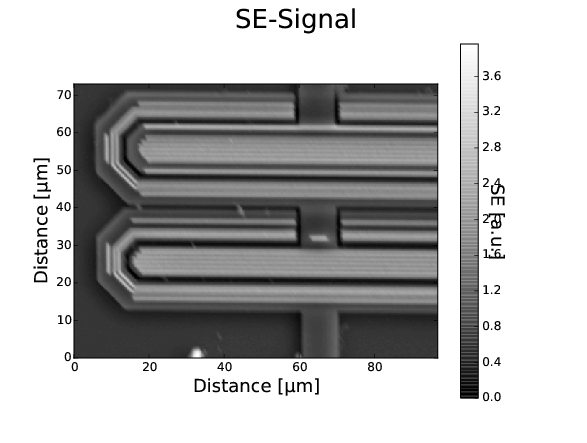
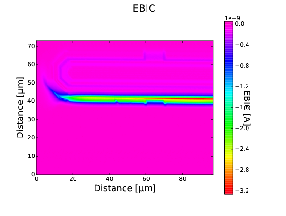
Gate Protection Diode EBIC Picture
MOSFET
The picture is quite different for the power MOSFET. Since the channel region is close to the surface, it is easy to excite some EBIC current. However, it looks like this strong response is limited to the transistors drift region, which is lightly n-doped.
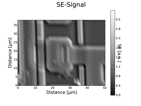
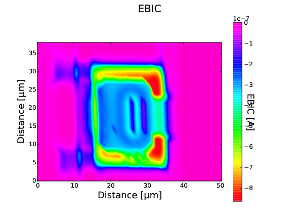
MOSFET EBIC Picture
Further Measurements
- A detailed analysis of the protection diode/gate leakage. It should be possible to separate the two Z-diodes in series and maybe the gate leakage current.
- Separate the body diode current from the reverse channel current.
- Redo the Forward- and Output Characteristics measurement and identify the source of mismatch. For example, check how an active elctron beam changes \(V_{\text{th}}\).
- Measure the maximum drain-source voltage \(V_{DS}\), which might even be on the order of 120 V. This measurement might be done destructively, or maybe by analyzing gate and drain leakage current. Then redo the full transistor measurement (Caution: power limit).
- Try to derive a model according to [1].
Bibliography
- [1] C.W. Tang, K.Y. Tong: A compact large signal model of LDMOS (Online) DOI:10.1016/S0038-1101(02)00238-1