
The aim of this measurement was to determine the current-voltage characteristics of a InN-thin film that was deposited on both, a Si- and a glass substrate with plasma-induced Atomic Layer Deposition (ALD). The measurement was performed with the four-wire method which is thoroughly described here. A picture of the samples can be seen below:
Drift regime: A thin film can be considered to be a 2-dimensional system. It is common to use the square sheet resistance $R_S$ to describe the electrical properties of such a system,
\begin{equation} R_S=\frac{\pi\cdot U}{\ln(2)\cdot I}, \end{equation}
with the current I and the voltage U. It is closely related to the resistivity $\rho$ and the sample thickness $t$ (20 nm):
\begin{equation} R_S=\frac{\rho}{t} \end{equation}
Furthemore, the temperature-dependent resistance needs to be taken into account. The behaviour can be obtained by looking at the electron ($n$) and hole concentration ($p$) of an intrinsic semiconductor, which are equivalent to the square-root of the intrinsic carrier concentration $n_i$ according to the law of mass action:
\begin{equation} n=p=n_i=\sqrt{N_c N_v}\cdot e^{-\frac{E_g}{2 k_B T}} \end{equation}
This equation links the band gap $E_g$ to the carrier densities. The effective electron ($N_c$) and hole concentrations ($N_v$) are also weakly temperature-dependent but this can be neglected in the measured temperature range. The final step is the relationship between the electrical conductance $\sigma$ and the carrier densities:
\begin{equation} \sigma=n e_c \mu_n +p e_c \mu_p=(\mu_n+\mu_p) e_c e^{-\frac{E_g}{2 k_B T}}, \end{equation}
with the elementary charge $e_c$. This means that the sheet resistance must show an exponential temperature-dependence acording to:
\begin{equation} R \propto e^{\frac{E_g}{2 k_B T}} \end{equation}
This means that a fit of $ln(R_S)$ vs $\frac{1}{T}$ should give an estimate for the band gap of the measured semiconductor.
Variable-range-hopping (VRH): However, the conclusions above were drawn under the assumption that diffusion is the main transport mechanism in the measured semiconductor. VRH is another model which describes the behaviour of semiconductors at lower temperatures:
\begin{equation} R=R_0 \cdot \exp\left(\left(\frac{T_0}{T}\right)^{\frac{1}{d+1}}\right), \end{equation}
with a typical temperature $T_0$ and the dimension $d$. In our case, a sample thickness of 20 nm satisfies the conditions for a 3d-system in this model.
The python code below uses a Keithley sourcemeter (SMU26xx-series) to perform four-wire measurements on the samples. Each measurement is repeated ten times to obtain a mean value and a standard deviation for an error estimate.
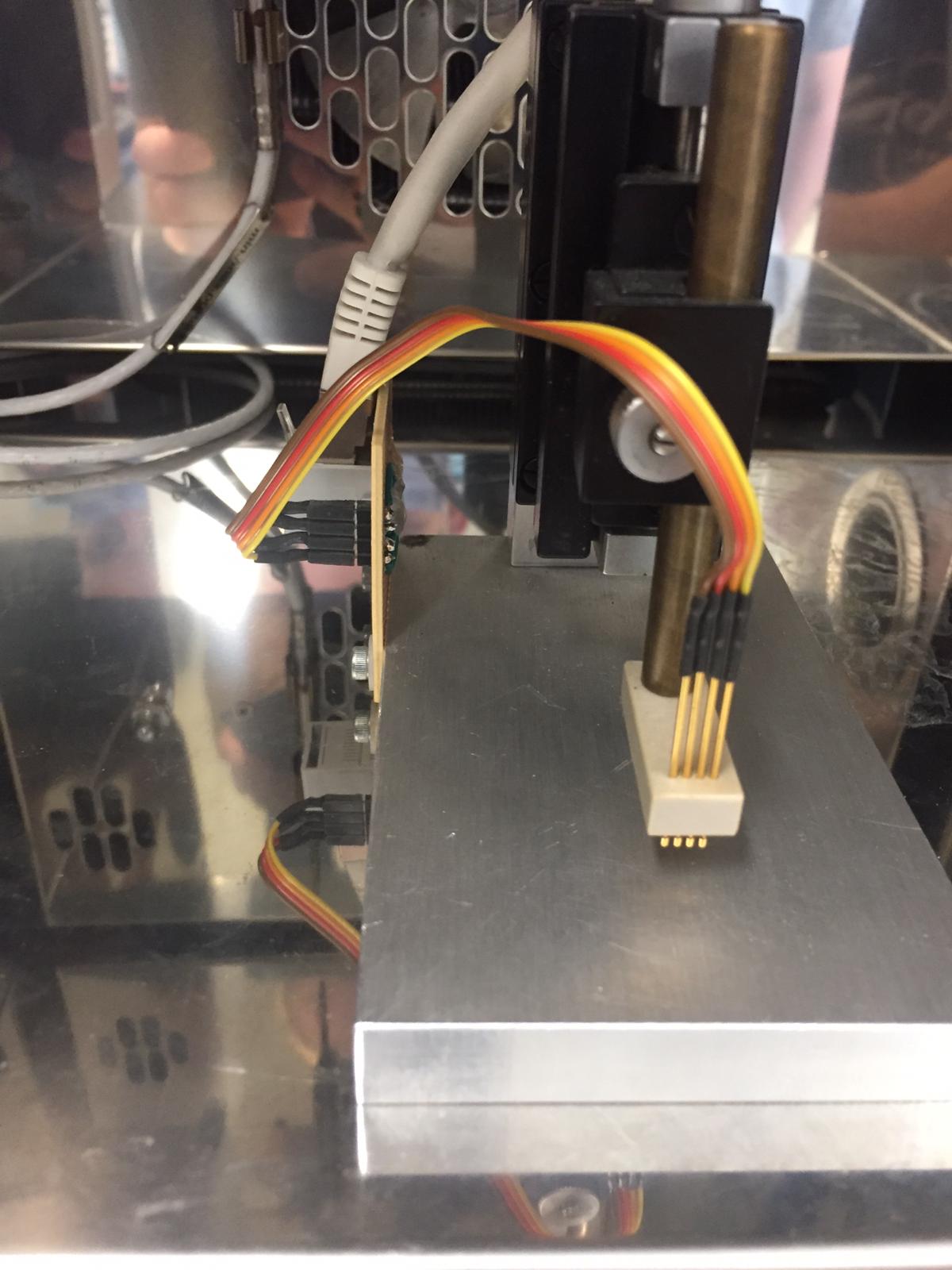
The samples were positioned in a climate chamber of type voetsch VT4002. Before starting the temperature sweep from 8 to 40 °C, some sample measurements were made at room temperture to ensure that the sample was properly connected to the measurement device. Due to the characteristics of the temperature-control mechanism, the value at the lowest temperature was excluded from the experiment to avoid unsound datapoints. The measurement device in the climate chamber can be seen in the figure below:
After ensuring that the samples were properly connected, the temperature sweep was started. The resulting resistivities for the thin films on both substrates are shown below:
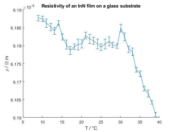
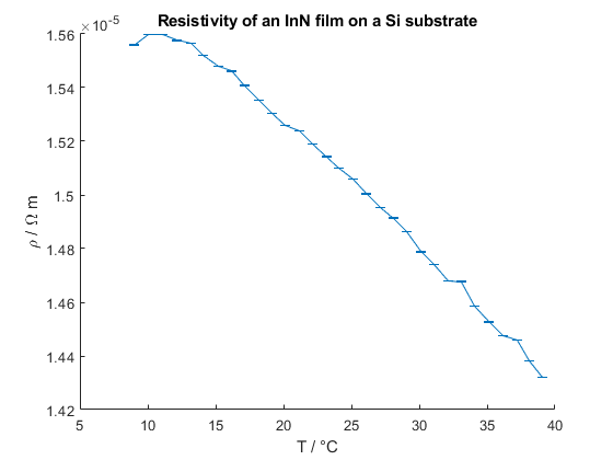
As can be seen, neither of the samples show a clear exponential behaviour. Nevertheless, the data from the Si-substrate was fitted to both, the drift model and the VRH-model:
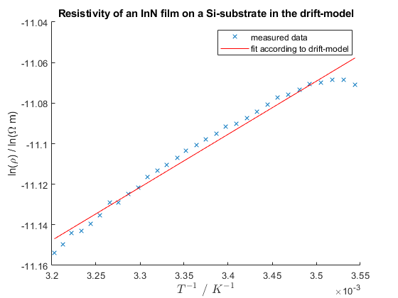
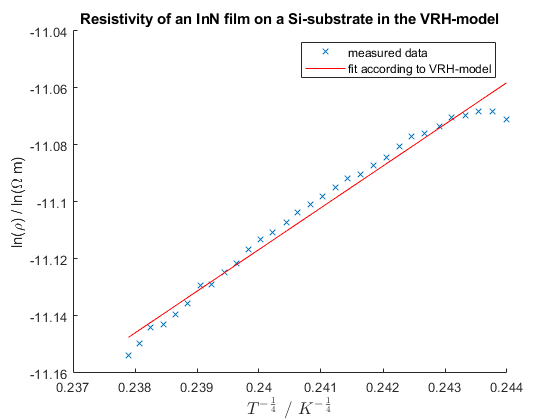
The calculation in the drift model results in a band gap of $E_g=0.045~eV$. A similar analysis of the steeper region in the data from the glass-substrate results in $E_g=0.07~eV$. The main idea behind the second analysis was that there might be a change in the dominant transport mechanism from VRH to drift at a temperature of about 30 °C. Still, both values are well below the literature value for the band gap of InN, which lies around 0.7 eV. It is also possible that the deposition of the thin film was corrupted by leaks in the vacuum system, which could have led to the formation of InO. However, InO has a band hap around 3 eV. The discrepancy between the measured values and the expected band gaps suggests that either the drift model is not applicable in this temperature regime or that the thin film is corrupted in a yet inexplicable way. Furthermore, the existence of a systematic measurement error must be considered. The fitted value for $T_0$ was around 14600 K. No literature value could be found for further comparison.
In order to clarify the obtained results, another measurement of equivalent samples should be performed. If the $\rho-T$-behaviour of the thin film on the glass substrate can be reproduced, a deeper analysis of the interplay between substrate and thin film would be necessary. Furthermore, the thin film itself should be examined to clarify its composition, this could be achieved with Rutherford-backscattering or other suitable methods.