PHT.301 Physics of Semiconductor Devices
|
|
PHT.301 Physics of Semiconductor Devices | |
|
|
MOSFET Gradual Channel ApproximationThe object of this calculation is to find an expression for the drain current as a function of the gate voltage and the drain voltage, $I_D(V_G,V_D)$. Recall from the discussion of a MOS capacitor that mobile charge appears at the semiconductor-oxide interface when the gate voltage $V_G$ minus the body voltage $V_B$ is greater that the threshold voltage $V_T$. Below the threshold voltage the MOS capacitior is in depletion and there are no mobile charge carriers. Above the threshold voltage the MOS capacitor is in inversion and the concentration of mobile electrons is linearly proportional to $V_G-V_B-V_T$, \[\begin{equation} Q_{\text{mobile}} = \begin{cases} 0, & \mbox{for } V_G-V_B < V_T \\ -C_{\text{ox}}(V_G-V_B -V_T) & \mbox{for } V_G-V_B > V_T \end{cases} \end{equation}\]Here $C_{\text{ox}}=\frac{\epsilon_r\epsilon_0}{t_{\text{ox}}}$ is the capacitance of the oxide per area, $\epsilon_r$ is the relative dielectric constant, $\epsilon_0$ is the permeativity constant, and $t_{\text{ox}}$ is the thickness of the gate oxide. If a drain voltage is applied and the source and the body are shorted, the voltage varies along the channel $V_{ch}(y=0)=0$, $V_{ch}(y=L)=V_D$. Consequently, the charge density in the inversion layer varies along the channel. In this calculation we assume that $V_G-V_{ch}(y) > V_T$ throughout the channel so that there is a finite mobile charge density everywhere in the channel. Under these conditions, the depletion width is constant everywhere and the charge density along the channel of an n-channel MOSFET is, \[\begin{equation} Q(y) = -en_s(y)=- C_{ox}(V_G-V_{ch}(y)-V_T). \end{equation}\]Here $-e$ is the charge on an electron and $n_s$ is the sheet charge in electrons/m². Ohm's law states that the current density is proportional to the electric field, \[\begin{equation} j_y=ne\mu_nE_y. \end{equation}\]Here $n$ is the electron density in electrons/m³ and $\mu_n$ is the electron mobility. The current in the channel is obtained by multiplying the current density with the corresponding area, where $Z$ is the width of the device and $t$ corresponds to the thickness of the channel. \[\begin{equation} I_D = Ztj = Ztne\mu_nE_y \end{equation}\]Using the relation between the sheet charge at the interface and the concentration of electrons $n_s = nt$ one gets the following expression: \[\begin{equation} I_D = Ze\mu_nn_s(y)E_y(y) \end{equation}\]The product $n_s(y)E_y(y)$ is a constant as a function of $y$. The sheet charge decreases near the drain so the electric field increases near the drain. The sheet charge can be expressed by the following equation using the expression for the charge in the inversion layer from above. \[\begin{equation} n_s(y) = -\frac{Q(y)}{e} = \frac{C_{ox}(V_G-V_{ch}(y)-V_T)}{e} \end{equation}\]By inserting this expression for the sheet charge into the formula for the current one obtains, \[\begin{equation} I_D = Z\mu_nC_{ox}(V_G-V_{ch}(y)-V_T)E_y. \end{equation}\]The electric field is minus the derivative of the potential, $E_y = -\frac{dV_{ch}}{dy}$. Substituing this in yields, \[\begin{equation} I_D = - Z\mu_nC_{ox}(V_G-V_{ch}(y)-V_T)\frac{dV_{ch}}{dy} \end{equation}\]The electrons are moving towards the drain so the current is in the $-y$ direction. It is conventional to take this as a positive drain current so we will insert a minus sign in the formula at this point. \[\begin{equation} I_D = Z\mu_nC_{ox}(V_G-V_{ch}(y)-V_T)\frac{dV_{ch}}{dy} \end{equation}\]Solving this first order differential equation for $V_{ch}$ yields, \[\begin{equation} V_{ch}(y) = V_G-V_T-\sqrt{(V_G-V_T)^2-\frac{2I_Dy}{Z\mu_nC_{ox}}}. \end{equation}\]The $y$-component of the electric field along the channel is, \[\begin{equation} E_y = -\frac{dV_{ch}}{dy}=-\frac{I_D}{Z\mu_nC_{ox}\sqrt{(V_G-V_T)^2-\frac{2I_Dy}{Z\mu_nC_{ox}}}}. \end{equation}\]The voltage, electric field, and charge density are plotted below. This model is only valid if the drain voltage is less then the saturation voltage.
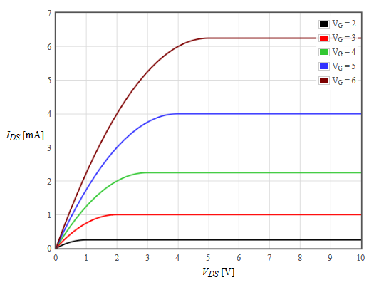
One can now integrate both sides from $y=0$ over the channel length to $y=L$ and from $V_{ch}=0$ to $V_{ch}=V_{D}$. \[\begin{equation} \int_{0}^{L} \! I_D \,\mathrm{d}y = \int_{0}^{V_{D}} \! Z\mu_nC_{ox}(V_G-V_{ch}(y)-V_T) \, \mathrm{d}V \end{equation}\]The current flowing from source to drain is constant everywhere so the integration of the left side just gives a factor of $L$. On the right side the voltage is integrated. The gate voltage $V_G$ and the threshold voltage $V_T$ are just constants, so the whole integration yields the following expression for the drain current in terms of voltage: \[\begin{equation} \boxed{I_D = \frac{Z}{L}\mu_nC_{ox}\Biggl\lbrack (V_{G}-V_T)V_{D} - \frac{V_{D}^{2}}{2} \Biggr\rbrack } \end{equation}\]This formula provides the desired relation between drain current $I_D$ and $V_{D}$ (valid until pinch-off occurs at the drain). The corresponding curves to this formula are plotted in the following figure.
The current in the saturation region $I_{sat}$ is the current that appears in the linear regime at pinch-off. At this point, $dI_{D}/dV_{D} = 0$. This condition can be used to determine the voltage $V_{sat}$ at pinch-off, \[\begin{equation} \frac{dI}{dV_D} = \frac{Z}{L}\mu_nC_{ox}\Biggl\lbrack (V_G-V_T)-V_D \Biggr\rbrack = 0. \end{equation}\]This condition is only met, if the expression inside the square brackets is zero. Thus, the saturation voltage is, \[\begin{equation} V_{sat}=(V_G-V_T) \end{equation}\]The saturation current can now be determined by substituting $V_{sat}$ into the expression for the formula for the current in the linear regime, \[\begin{equation} I_{sat} = \frac{Z}{2L}\mu_nC_{ox}(V_G-V_T)^{2} \end{equation}\]The saturation current $I_{sat}$ does not depend on the drain voltage $V_{D}$ in the saturation region. In this regime a MOSFET acts like a voltage controlled current source. If $V_G < V_T$, there are no mobile charge carriers in the channel and the MOSFET is in the cutoff regime. A closer look at pinch-offAs the drain voltage approaches the saturation voltage, the gradual channel approximation predicts that the mobile charge density goes to zero and the electric field diverges. This condition is called pinch-off. The portion of the channel that is pinched off is essentially fully depleted and the derivative of electric field is related to the doping density by Gauss's law, $\frac{dE_y}{dy}=-\frac{eN_A}{\epsilon_r\epsilon_0}$. Here $N_A$ is the concentration of acceptors. In the saturation regime we can break the channel into two parts. In the part that is not pinched off $(0 < y < y_p)$, the gradual channel approximation is used. In the pinched-off region $(y_p < y < L)$, Gauss's law is used. This results in the condition, \begin{equation} \frac{dE_y}{dy}(y_p) = -\frac{I_D^2}{Z^2\mu_n^2C_{ox}^2\left((V_G-V_T)^2-\frac{2I_Dy_p}{Z\mu_nC_{ox}}\right)^{3/2}}=-\frac{eN_A}{\epsilon_r\epsilon_0}. \end{equation}The voltage in the channel at $y_p$ is, \begin{equation} V_{ch}(y_p) = V_G-V_T-\sqrt{(V_G-V_T)^2-\frac{2I_Dy_p}{Z\mu_nC_{ox}}}. \end{equation}The voltage across the pinched off region is, \[\begin{equation} V_{po} = -\int\limits_{y_p}^{L}E_ydy = \frac{eN_A}{2\epsilon_r\epsilon_0}(L^2-y_p^2). \end{equation}\]The voltage drops across the two parts must add to be the drain voltage $V_{ch}(y_p)+ V_{po} = V_{D}$, \[\begin{equation} V_G-V_T-\sqrt{(V_G-V_T)^2-\frac{2I_Dy_p}{Z\mu_nC_{ox}}}+\frac{eN_A}{2\epsilon_r\epsilon_0}(L^2-y_p^2)=V_D. \end{equation}\]This last equation and the equation for $\frac{dE_y}{dy}(y_p)$ can be solved numerically to determine $y_p$ and $I_D$. The drain current will increase in the saturation regime in this model. Shorter gate lengths and lower body doping results in more channel length modulation. |