
n-channel JFET with metal contacts for Source and Drain
p-channel JFET with metal contacts for Source and Drain
Basics
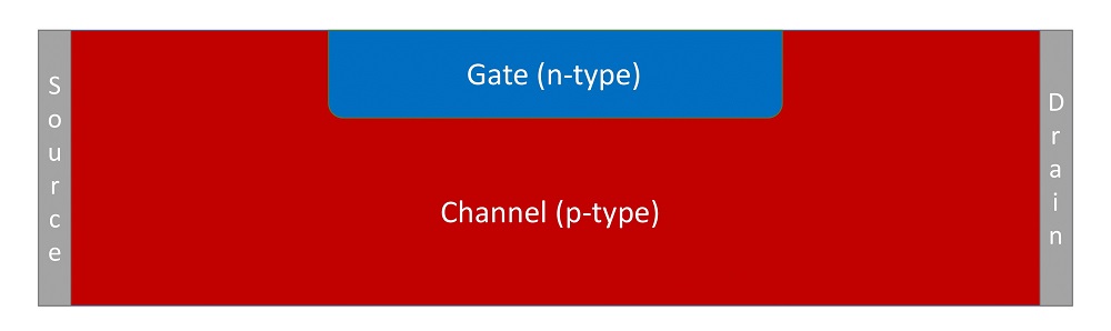
There are two types of JFETs. They can either be n-channel or p-channel, this refers to the doping of the bulk material. On both ends of the channel material there are contacts called Source and Drain. Between Source and Drain there is the Gate which is a differently doped region. The picture below shows both a n-channel and a p-channel JFET. The Gate region forms a pn junction with a depletion region. The width of this depletion region can be controlled with the voltage that is applied to the Gate.
Measurements
The following measurements were perfomrmed with this JFET using a Keithley 2600 Series Sourcemeter:
Characterization of the JFET
In order to identify the channel type of this JFET one can use the pn junction as an indicator. If one applies a positive voltage to the Gate of a n-channel JFET and measures the current, the result will show the behaviour of a forward biased diode. The opposite holds for the p-channel JFET. The python code for this measuremnt was taken from the webpage Diode Measurements with a Sourcemeter and adapted.
This script requires the Keithley 2600 Python library which must be saved in the working directory.
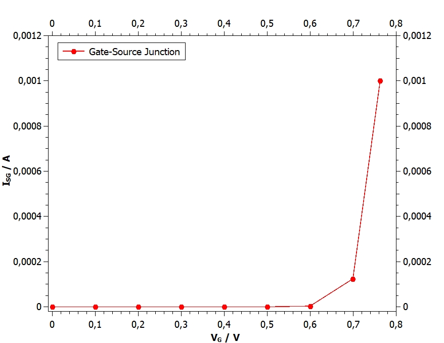
For this measurement the B-channel of the Keithley was connected to the Gate and the A-channel was connected to the Source. With the B-channel a positive voltage was applied to the Gate and the A-channel on the Source measures the current. As can be seen in the measurement below the Junction behaves like a forward biased diode, thus it can be concluded that the measured JFET is a n-channel JFET.
Data
The measured data of the characterization of the pn junction can be found in the box below.
Gate Voltage at pintch-off
In order to measure the pintch-off behaviour of the JFET the python program transistor_n_channel was used. The script uses channel A of the Keithley measure the current and generate Voltage and the B-channel applies a voltage.
This script requires the Keithley 2600 Python library which must be saved in the working directory.
For this measurement the B-channel was connected to the gate in order to apply a negative gate voltage to find the value for the gate voltage at pintch-off. The A-channel was connected to the Drain and the Source to the common Ground. This measurement was done for four different Source-Drain Voltages.
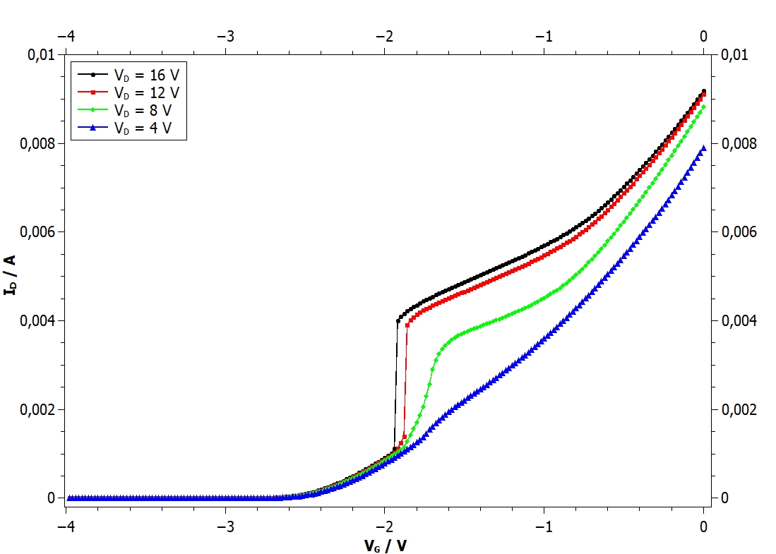
The higher the Drain Voltage the higer the Drain Current in the beginning. With incresing negative $\text{V}_{G}$ the channel gets smaller and smaller until at $\text{V}_{G} = -2\,\text{V}$ the current that can flow through the channel is striktly limited. The current for $\text{V}_{D} = 4\,\text{V} $ shows almost no no effect at this point.
Data
The measured data for the pintch-off behaviour is listed in the textbox below. The first colum represents the Gate voltage in V,
the second column the $\text{I}_{D}$ for $\text{V}_{D} = 4\,\text{V}$, the third for $\text{V}_{D} = 8\,\text{V}$, the fourth for $\text{V}_{D} = 12\,\text{V}$ and the fifth for $\text{V}_{D} = 16\,\text{V}$ .
In order to find a value for the $\text{V}_{G}$ at pintch-off, the equation that describes the behaviour of the $\text{I}_{D}$ in the limit of the linear regime was closely examined. This equation was taken from n-channel JFET.
\begin{equation} I_D=I_p\left[\frac{V_D}{V_p}-\frac{2}{3}\left(\frac{V_{bi}+V_D-V_G}{V_p}\right)^{3/2}+\frac{2}{3}\left(\frac{V_{bi}-V_G}{V_p}\right)^{3/2}\right], \end{equation}As can be seen in this equation, there is a power of $3/2$ involved. Hence to be able to fit the IV curves linearly the $\text{I}_{D}$ values were taken to the power of $2/3$. This way it was possible to apply a linear fit in the linear region close to the pintch-off point and with those parameters the values for $\text{V}_{G}$ at the pintch-off point for each $\text{V}_{D}$ could be calculated.
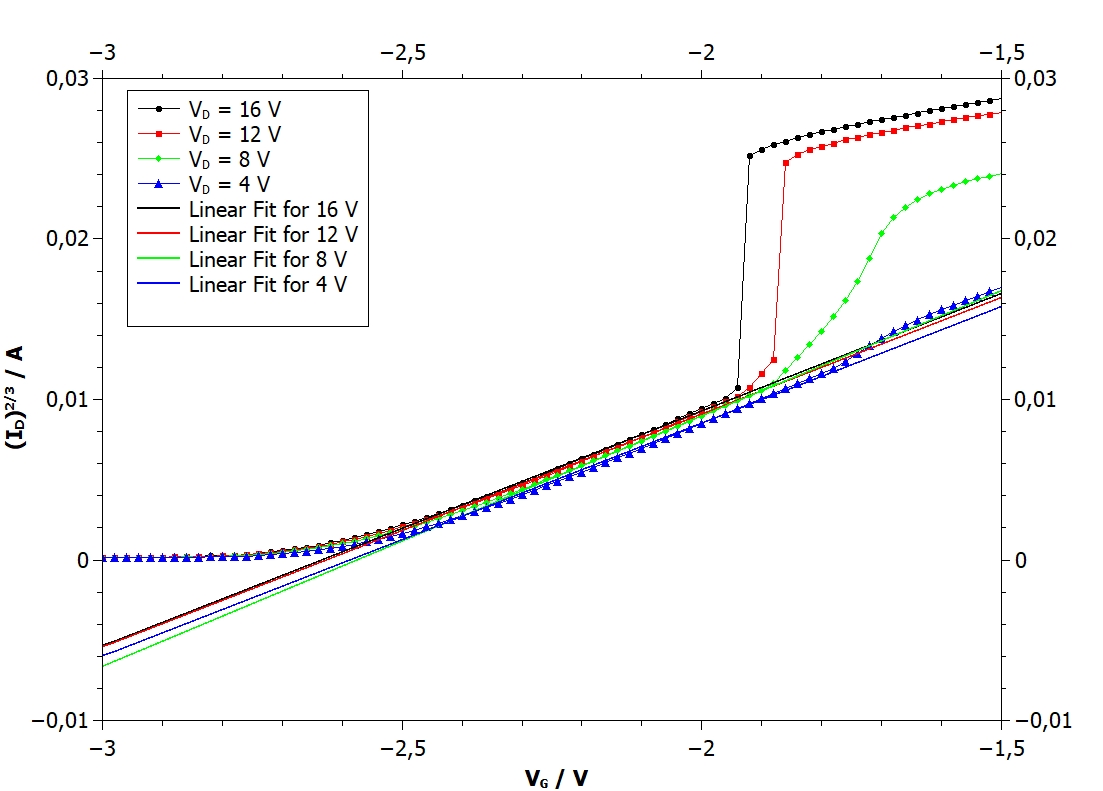
The calculated values for $\text{V}_{G}$ are the following:
Possible extensions of these measurements