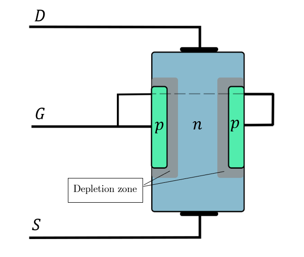
A JFET is a common transistor, which consists in a configuration of three doped semiconductors with three electrical pins.
The one used in this exercise is a n-channel, whose main part is made up of a n-doped semiconductor, joint with two smaller p-type ones (see Fig.1).
The gate pin (G) is connected to those p-type semiconductors, and the n-type is connected to a source (S), usually grounded, and to a drain pin (D).
When a certain voltage is set between S and D pins, electrons flow from the source to the drain, causing the depletion zone between semiconductors to vary accordingly.
This way, the current that goes trhough can be controlled by changing the width of the depletion zones.
Fig.1: Composition of a n-channel JFET
This experience consisted in several measurements of inputs and output characteristis of a JFET transistor, as well as the temperature dependence of its resistance.
The goal is to indentify the main properties of the JFET and the dopant concentration throughout the resistance measurement.
Equipment Used
Sourcemeter
For the voltage supply and for the electrical measurements the Keithley 2636A Series Sourcemeter was used.
This sourcemeter has two separate channels which are necessary to fully operate the JFET.
To communicate with the device, already existing python scripts were used and slightly edited.
The example python scripts as well as the Keithley 2600 Pyhton library can be found here:
Diode Measurements with a Sourcemeter.
JFET
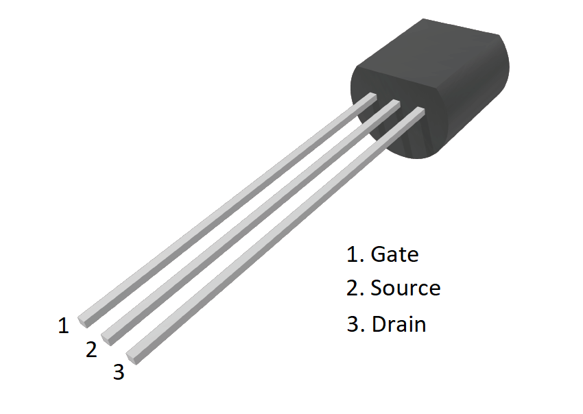
For the measurements of the transistor characteristics a JFET BF256B from the company Fairchild was employed.
The contact pins are as labled in Fig.2.
Fig.2: JFET BF256B contact pins
Climate Chamber
To determine the dopping concentration of the transistor the following Vötsch VT4002 climate chamber was used, this allowed the transistor to be stablished at a certain temperature.
Experimental Setup and Measurements
Diode characteristics of the JFET
To identify the JFET as a n-Channel type, the source current IS was measured while applying a forward bias voltage VGS
between the gate and the source and sweeping it. The curve behaved as assumed for a JFET with a n-Channel. The same was done between the gate and the drain
contact of the JFET with respectively ID and VGD. For this setup, only one channel (Channel A) of the sourcemeter was necessary.
It's also interesting to measure the gate current IG which was done while the same script was running. For this setup, the other channel (Channel B) of the
sourcemeter was used.
The following python script was implemented for this routine:
This current-voltage behavior of the diode can be described by the diode equation.
For more information see PN diode IV characteristics.
\[ \begin{equation}
\large I = I_S\left(\exp\left(\frac{eV}{k_BT}\right) - 1\right)\hspace{0.5cm}\text{[A]}
\end{equation} \]
Gate voltage and deplation zone
The next step was to measure the source-drain current ISD while increasing the source-drain voltage VSC for
different gate-drain voltages VGS.
For this experiment, both channels of the sourcemeter had to be used. Therefore the python script of a report from another group
N-channel JFET, (paragraph "Output Characteristics")
was provided and further modified.
Resistance dependence with temperature
For this section of the experiment, the climate chamber was sweeping the temperature while measuring the electrical resistance of the transistor.
In order to do so, a python script slightly modified of the one provided in the website
Vötsch VT4002 climate chamber was used.
Results and Discussion
Diode characteristics of the JFET
As it can be seen in Fig.3 and Fig.4, Gate-Drain curves and Gate-Source curves are close to identical.
It can thus be concluded that there is no doping gradient in the n-channel.
Fig.3: Gate Drain & Gate Source Curve
Fig.4: Gate Drain & Gate Source (log plot)
To compare the diode behavior between the Gate and Source to the Diode Equation another measurement with a higher sweep range was taken.
Fig.5 shows that the curve only follows the exponential behaviour in a rather small region, therefore only this part was taken into account for the fit (solid red line).
For the fit a constant temperature of $T=$295.5 K was used.
For the lower voltages this could be the case because of the accuracy of the sourcemeter, since the current was relatively constant at a current
of 1.1 mA in the range of 0 to 0.5 $V_{GD}$, which was truncated in the plot for a better visual representation.
The flattening at higher voltages could be caused by the device heating up with and the strong temperature dependency of the function.
As results following values for the dark saturation current $I_S$ and the ideality factor $n$ determined:
$I_S = \text{4.79·10}^{-15}$ A $n = 1.142$
While the value for n seems plausible, since it normally lies between 1 and 2, the value for the saturation value is rather small.
Fig.5 Diode characteristic and diode equation fit of the JFET
Gate voltage and depletion zone
These measurements were mainly done to find an operating voltage for the measurements in the temperature chamber.
Fig.6 clearly shows the linear region at low and the saturation region at higher source-drain voltages $V_{DS}$ for different gate voltages, while in Fig.7 only the linear region is represented.
For the further measurements in the temperature chamber a gate voltage at $V_G=0$ and a source-drain voltage $V_{SD}=0.2$ was chosen since the resistance in the n-channel was chosen to be as small as possible.
Fig.6: Linear and saturation region at differnet gate voltages of an JFET
Fig.7: Linear region at differnet gate voltages of an JFET
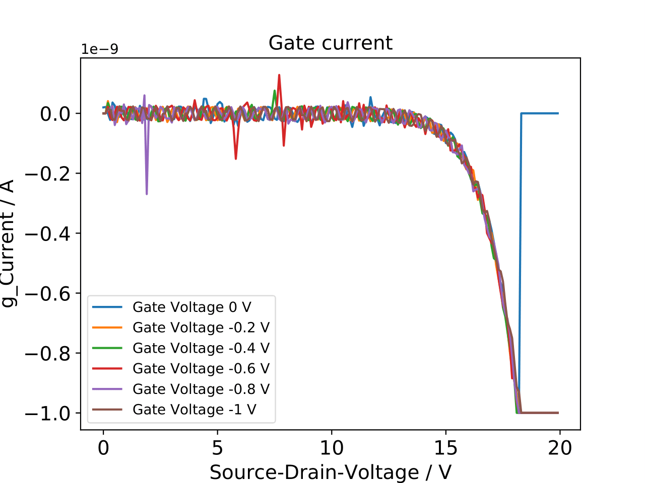
Gate current
Results obtained with Channel B for the gate current are shown in Fig.8
Fig.8: Gate-Drain current curve for diffetent Gate voltage values
The gate current plot refers to the current formed between the gate and the drain, therefore it's just a pn-junction. A graph similar to the diode (Fig.3) was expected to happen with different exponential growings associated with the different gate voltages, but instead a break down happening at the same value is obtained. We encourage the next students to take a closer look into this behaviour.
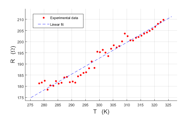
Temperature dependence of resistance, determination of $N_d$
Results obtained with the climate chamber are shown in Fig.9
Fig.9: Experimental resistance $R$ as a function of tempreature $T$
An increase in resistance is observed with temperature. In this regime, the transistor acts just as a resistor where $n=N_d$.
The change in dopant concentration is negligible for these energies, nonetheless phonon scattering lowers the mobility of the carriers. One can note an anomalous noise for the first values.
Further reasearch on this behavior and repetition of the measurement is encouraged. The linear fit shows an equation for resistance $R(T) \approx 0.71 T -21.3 \: [\Omega]$ . The fit has a correlation coefficient of $r^2=0.95$.
Resistance can be expressed as $R(T)=\frac{1}{\sigma (T)} \frac{l}{A}$ where $\sigma$ is the conductivity and $l,A$ the length and cross area, respectively. If we set a reference temperature $T_0$ and $R_0=R(T_0)\:, \sigma _0=\sigma (T_0)$ then:
$$
\frac{R(T)}{R_0}=\frac{\sigma _0}{\sigma (T)} \to \frac{\sigma (T)}{\sigma _0}=\frac{R_0}{0.713 T -21.30}
$$
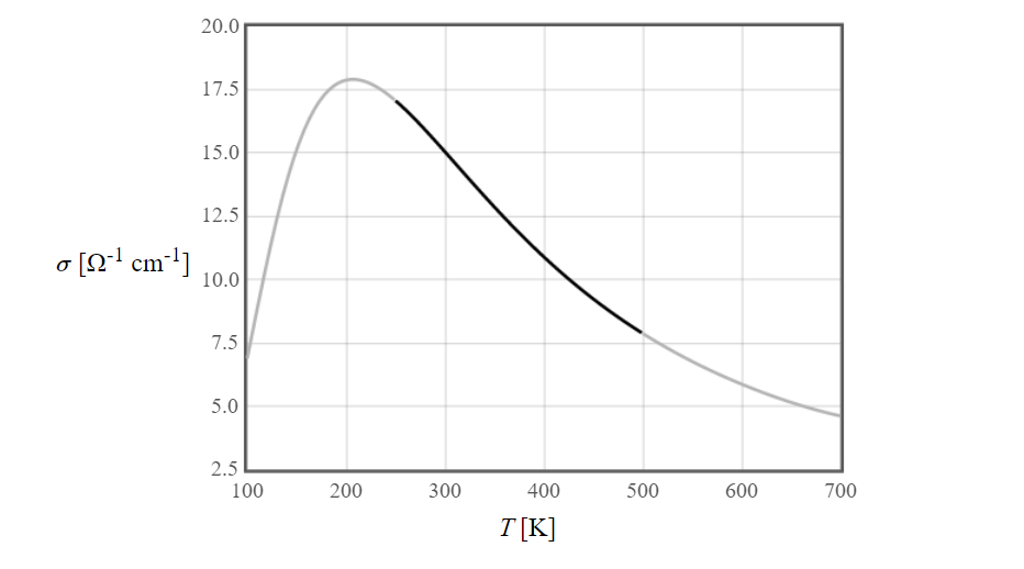
Choosing $T_0=311 \:\text{K}$ and $R_0=200.6 \:\Omega$, we expect a slope of the function of approximately $0.034 \sigma _0$ around $T_0$. In Peter Hadley's Physics of Semiconductor Devices lecture webpage, further information about mobility of carriers can be found.
In specific, we can relate this obtained slope with density of dopants using the tool in the webpage Electrical conductivity of silicon , finding a resulting value of approximately $N_d \approx 1.35·10^{17} \text{cm}^{-3}$. Theoretical fit is shown in Fig.10