A JFET transistor has three different pins. In a n-channel JFET, like the one used in this laboratory, Source (S) and Drain (D) are connected by a n-doped semiconductor. The Gate (G) contacts a p-doped zone, that surrounds the n-channel. This design creates a pn junction, which depletion zone width is controlled by the voltage applied to the Gate. This way the width of the conducting channel between Source and Drain and therefore the resistance of the JFET can be controlled. In this laboratory the output characteristic, the Drain current over the Source-Drain voltage, as well as the diode behaviour between Gate and both Source and Drain were examined. For a theoretical analysis of the output characteristic see the page n-channel JFET from the course "Physics of Semiconductor Devices" by Prof. Hadley.
As part of this laboratory, these measurements were performed on an n-channel JFET with a Keithley 2600 Series Sourcemeter:
Diode Behaviour
First the two different diodes, formed between Gate-Source and Gate-Drain, were measured with the following diode program. The python code used for the diode measurement was changed and adopted from the webpage Diode Measurements with a Sourcemeter.
This script requires the Keithley 2600 Python library which must be saved in the working directory.
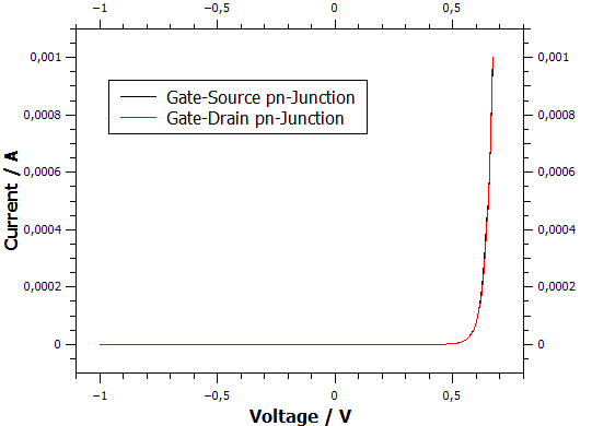
For this measurement, Gate contact was connected to Channel A and Ground was first connected to Source and then to Drain. The results for the two different diodes are very similar and prove that it is indeed a n-channel JFET. This can be seen by the characteristic line for a forward biased Diode. At about 0.6 V the break through voltage is reached and a significant current starts to flow. So the pn-junction is connected in forward bias which applies a positive voltage on the p doped Gate and a corresponding negative voltage on the n doped Source and Drain. As the two different measurements show almost identical results, it can be concluded that there is no doping gradient in the n-channel.
Data
The measured data for the pn-junction between Gate and Source is given in the textbox below. The first column is voltage in V and the second column is current in A.
Output Characteristic
The output characteristic for the transistor was measured with a different script. The following script uses both channel A and channel B to sweep over the Drain Source voltage and the Gate voltage. For this specific script channel A was connected to Drain, channel B was connected to Gate and Ground was connected to Source.
In the next figure an overview of the output characteristic is shown for different Gate voltages from 0 to -7 V.

As the Drain current shoots up to the maximum allowed current straight away for applied voltages from -1 V to -5 V, for this particular transistor the Gate voltages are too low to achieve pinch off. So another sweep was performed but this time with slightly varied parameters as the Gate voltage was set between -6.0 V and -6.7 V.

This time the current does not shoot up straight away, but the saturation current was not reached either. This is the case as the used transistor was a power transistor which is set up for much higher currents than the other measurement set-up. Therefore, the saturation regime cannot be reached with this transistor and this measurement set-up. On the webpage n-channel JFET there are two different formulas for the Drain current for the linear and the saturation regime. In this laboratory the saturation regime was not reached, so the current $I_p$ cannot be fitted easily because it is multiplied with another fit parameter, namely $V_p$. To get values for $I_p$, $V_p$ and $V_{bi}$ data for both regimes is needed and both fits have to be performed.
Data
The measured data for the output characteristic is given in the textbox below. The first column is the applied Source-Drain voltage in V,
all further columns give the data for different Gate voltages in the following order: -6.0 V, -6.1 V, -6.2 V, -6.3 V, -6.4 V, -6.5 V, -6.6 V and -6.7 V.
N-Channel Resistance measurement
For the resistance measurement a slightly varied script was used which calculates and plots the resistance directly.
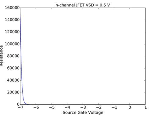
As the applied voltage between Source and Drain as well as the current flowing is known, the resistance can be calculated. In the following figure the resistance in Ohm is plotted over the applied Gate voltage in Volts with a fixed Source Drain voltage of 0.5 V. For Gate voltages under 5 V the channel resistance is an the few Ohm regime. From 5 V upwards, the resistance starts to increase more strongly. As shown in the figure above, over 6.5 V the resistance increased rapidly as the pinch off voltage is approached.
Data
In the following textbox the applied Gate voltage is given in the first column in V whereas in the second column the calculated resistivity is given in Ohm.
Possible extensions of these measurements