![]()
PHY.K02UF Molecular and Solid State Physics
|
| |||
PHY.K02UF Molecular and Solid State Physics | ||||
Semiconductors are materials with a band gap $E_g < \text{ 3 eV}$ that, at low temperatures, separates the occupied electron states in the valence band from the empty electron states in the conduction band. The energy at the top of the valence band is called $E_v$, and the energy at the bottom of the conduction band is called $E_c$, $E_g = E_c - E_v$. At room temperature, some electrons are thermally excited across the band gap. This results in a few occupied electron states near the conduction band minimum and a few empty electron states near the valence band maximum. Consequently, only the states near the top of the valence band and the bottom of the conduction band are relevant for calculating most of the thermodynamic and electrical properties of a semiconductor.
Semiconductors are classified as having a direct band gap or an indirect band gap. In a direct band gap semiconductor, the minimum of the conduction band has the same value of $\vec{k}$ as the maximum of the valence band. For indirect band gap semiconductors, the minimum of the conduction band and the maximum of the valence band occur at different values of $\vec{k}$.
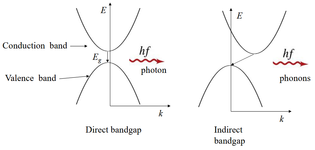
Two important applications for semiconductors are light-emitting diodes and solar cells. In a light-emitting diode, electrons are electrically injected into the conduction band while electrons are extracted from the top of the valence band. The electrons in the conduction band fall to the valence band and emit a photon of light. In this process, energy and momentum must be conserved.
$$\text{conservation of energy}\qquad E_c(\vec{k}_c) - E_v(\vec{k}_v) = E_g = hf_{\text{photon}}$$ $$\text{conservation of momentum}\qquad \hbar\vec{k}_c - \hbar\vec{k}_v= \hbar \vec{k}_{\text{photon}}$$The momentum of a visible photon $\hbar \vec{k}_{\text{photon}}$ is much smaller than the momentum of an electron in a $\vec{k}$-state on the Brillouin zone boundary. Consequently, an electron makes an almost vertical transition in these band diagrams from the conduction band at wave vector $\vec{k}_c$ to the valence band at wave vector $\vec{k}_v$ when it emits a photon. Therefore, semiconductors used in light-emitting diodes must have a direct band gap so that the electrons in the conduction band can fall directly down into the holes in the valence band. Forward-biased diodes of indirect bandgap semiconductors typically emit phonons instead of photons. The phonons can absorb the momentum needed when the electrons fall from a $\vec{k}$ state in the conduction band to a different $\vec{k}$ state in the valence band. This just heats up the crystal.
A solar cell works like a light-emitting diode in reverse. A photon with an energy larger than the band gap moves an electron from the valence band to the conduction band. This electron passes through an external circuit before returning to the valence band. Solar cells work with both direct band gap semiconductors and indirect band gap semiconductors because there are always empty states in the conduction band directly above occupied states in the valence band. The incoming photon just needs more energy than $E_g$ to lift an electron into the conduction band. The most commonly used semiconductor for solar cells is silicon, which has an indirect band gap.
The buttons below will allow you to load some simplified band structure diagrams of direct band gap and indirect band gap semiconductors. These diagrams only show the parts of the band diagrams near the top of the valence band and the bottom of the conduction band.
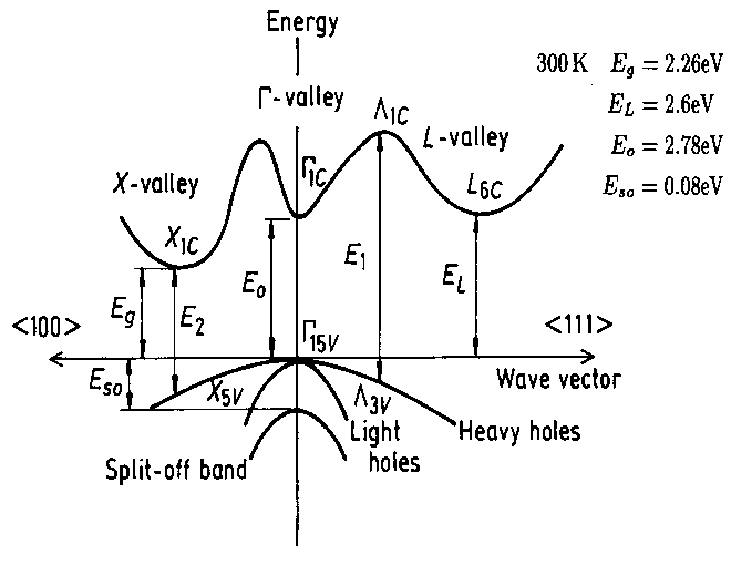
Simplified band structure of GaP. From NSM Archive.
Direct:
Indirect:
Often, additional minima are shown in the conduction band. If these minima are within a few $k_BT$ of the lowest minimum of the conduction band, electron states in these minima will become occupied as well. At room temperature, $k_BT\approx 25\text{ meV}$. Two bands are often degenerate at the top of the valence band at $\vec{k}=0$. These are called the light hole band and the heavy hole band. In addition, there is often another band with a maximum at $\vec{k}=0$ with a slightly lower energy called the split-off band.
The names 'light hole' and 'heavy hole' come from an approximation that is used to describe the $E\text{ vs. }k$ band structure near the top of the valence band and the bottom of the conduction band. In the simplest case, the minimum of the conduction band can be fit to a paraboloid,
$$E = \frac{\hbar^2(\vec{k}-\vec{k}_{c})^2}{2m_{e}^*}+E_c,$$where $E$ is the energy of an electron in the conduction band with wave vector $\vec{k}$, $\vec{k}_c$ is the wavevector at the conduction band minimum, and $m_{e}^*$ is called the effective mass of electrons in the conduction band. The effective mass determines the curvature of the paraboloid and is used to fit the parabola to the minimum of the conduction band, which must be determined with a band structure calculation. The effective mass can be determined from a band structure calculation of $E(\vec{k})$ by taking the second derivative,
$$\large m_{e}^* = \frac{\hbar^2}{\frac{d^2E(\vec{k})}{dk_x^2}\Big{|}_{\vec{k}_{c}}}.$$The band for free electrons was also parabolic so the density of states near the bottom of the conduction band will have the form of the free electron density of states,
$$D(E) = \frac{(2m_e^*)^{3/2}}{2\pi^2\hbar^3}\sqrt{E-E_c} .$$This is a good approximation for many direct band gap semiconductors, but indirect band gap semiconductors have multiple conduction band minima. For instance, silicon has a conduction band minimum in the [100] direction. By symmetry, there must be six mimina in the [100],[-100],[010],[0-10],[001],[00-1] directions. These minima are not isotropic paraboloids. More generally, the dispersion curve at a conduction band minimum can have the form,
$$E = \frac{\hbar^2(k_x-k_{cx})^2}{2m_{ex}^*}+\frac{\hbar^2(k_y-k_{cy})^2}{2m_{ey}^*}+\frac{\hbar^2(k_z-k_{cz})^2}{2m_{ez}^*}+E_c.$$Here $\vec{k}_c=[k_{cx},k_{cy},k_{cz}]$ is the position of the minimum. The effective mass can be different in the $x-$, $y-$, and $z-$directions. For the silicon minimum in the [100] direction, the effective mass in the $x-$direction is called the longitudinal effective mass $m_l$, and the effective masses in the $y-$ and $z-$directions are the same and they are called the transverse effective mass, $m_t$. By symmetry, for the minimum in the [010] direction, the effective mass in the $y-$direction is the longitudinal effective mass, while the effective masses in the $x-$ and $z-$directions are the transverse mass.
Even with multiple conduction band minima and different effective masses, the density of states near the conduction band edge grows as the square root of the energy,
$$D(E) = D_c\sqrt{E-E_c} = \frac{(2m_{\text{dos}})^{3/2}}{2\pi^2\hbar^3}\sqrt{E-E_c}.$$Here $m_{\text{dos}}$ is called the 'density of states effective mass' that takes into account the multiple minima and anisotropic form of the $E \text{ vs. }k$ paraboloid.
The top of the valence band is typically at $\vec{k}=0$ and can also be fit with a parabola. However, if we use the formula above for the effective mass, it turns out to be negative. One way to avoid this apparent paradox is to introduce the concepts of holes. Consider how we would calculate the electrical current density contributed by the electrons in the valence band. The current would be the charge of the electron $-e$, times the velocity $\vec{v}_{\vec{k}}$ of the electron in state $\vec{k}$ times the density of states $D(\vec{k}) = \frac{2}{(2\pi)^3}$ integrate over all of the filled states.
$$\vec{j} = \int\limits_{\text{filled states}}\frac{-2e\vec{v}_{\vec{k}}}{(2\pi)^3}d\vec{k}$$Integrating over the filled states is the same as integrating over all of the states in the valence band and then subtracting the contribution of the empty states.
$$\vec{j} = \int\limits_{\text{all states}}\frac{-2e\vec{v}_{\vec{k}}}{(2\pi)^3}d\vec{k} - \int\limits_{\text{empty states}}\frac{-2e\vec{v}_{\vec{k}}}{(2\pi)^3}d\vec{k}$$For every state $\vec{k}$ with a velocity $\vec{v}_{\vec{k}}$ in the band is a state $-\vec{k}$ with a velocity $-\vec{v}_{\vec{k}}$, so the integral over all states in the valence band is zero. The current density can be determined by just considering the empty states.
$$\vec{j} = \int\limits_{\text{empty states}}\frac{2e\vec{v}_{\vec{k}}}{(2\pi)^3}d\vec{k}$$Notice that two minus signs cancel, and in this final expression, it seems as if the charge associated with each electron state is $+e$. The empty states at the top of the valence band are called holes, and each is assigned a positive charge $+e$. The electrostatic energy of a positive charge is opposite that of a negative charge, so the effective mass of the holes is,
$$\large m_{h}^* = \frac{-\hbar^2}{\frac{d^2E(\vec{k})}{dk_x^2}\Big{|}_{\vec{k}=0}}.$$This simplifies the discussion of the properties of semiconductors significantly. Even though the electrons in a semiconducting crystal move through a periodic potential, we can describe the electrical and thermodynamic properties of the semiconductor as if the electrons in the conduction band act like free particles with an effective mass $m_e^*$ and the holes (empty states in the valence band) act like free particles with a positive charge $+e$ and an effective mass $m_h^*$. There are often two bands that meet at the top of the valence band with different curvatures. These are the light holes with effective mass $m_{lh}$, and heavy holes with effective mass $m_{hh}$. It is not proven here, but these effective masses are also the appropriate masses to use when calculating the acceleration of the electrons and holes under the influence of an externally applied electric field. Parameters such as $E_g$, $m_{l}$, $m_{t}$, $m_{lh}$, $m_{hh}$, and $m_{\text{dos}}$, for different semiconductors can be found in the NSM Archive
The density of states at the valence band also rises like a square root,
$$D(E) = D_v\sqrt{E_v-E}.$$Here the parameter $D_v$ takes the contributions of the light holes and the heavy holes into account.
The relevant part of the electron density of states of a semiconductor is close to the valence band and the conduction band. In three dimensions, the density of states of a semiconductor near the band gap is,
| $D(E) = \begin{cases} D_v\sqrt{E_v-E}, & \mbox{for } E\lt E_v \\ 0, & \mbox{for } E_v\lt E\lt E_c \\ D_c\sqrt{E-E_c}, & \mbox{for } E_c \lt E \end{cases}$ | 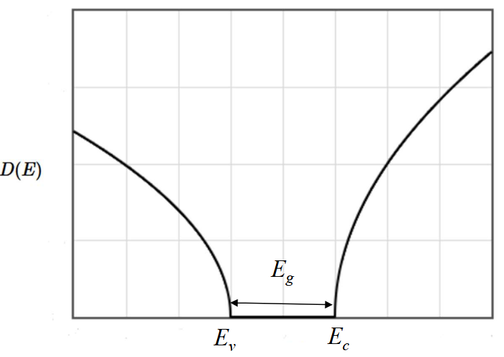 |
The density of states has been drawn for $D_c > D_v$. However, for some semiconductors $D_c > D_v$ and for some semiconductors $D_c < D_v$.
In two dimensions, the density of states of a semiconductor near the band gap is,
| $D(E) = \begin{cases} D_v, & \mbox{for } E\lt E_v \\ 0, & \mbox{for } E_v\lt E\lt E_c \\ D_c, & \mbox{for } E_c \lt E \end{cases}$ |  |
In one dimensions, the density of states of a semiconductor near the band gap is,
| $D(E) = \begin{cases} \frac{D_v}{\sqrt{E_v-E}}, & \mbox{for } E\lt E_v \\ 0, & \mbox{for } E_v\lt E\lt E_c \\ \frac{D_c}{\sqrt{E-E_c}}, & \mbox{for } E_c \lt E \end{cases}$ |  |
These forms for the density of states can be used to calculate the thermodynamic properties of semiconductors using the Boltzmann approximation.