Semiconductor Laboratory
|
|
Semiconductor Laboratory | |
|
|
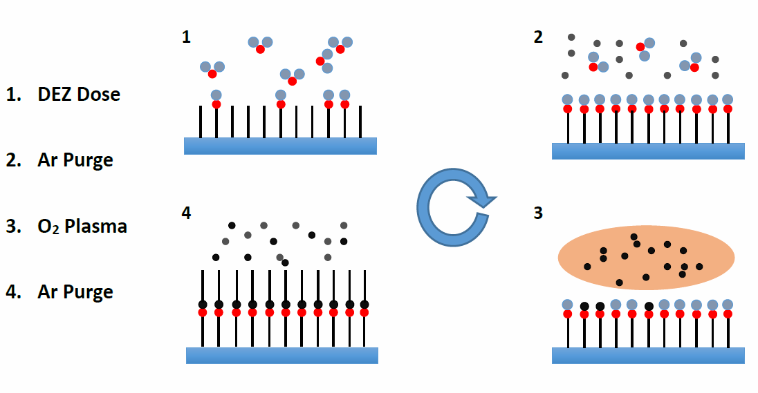
plasma-atomic layer deposition (Plasma-ALD)The scientific and technological interest in plasma-ALD is exponentially growing due to the high potentials of this technique. Plasma-ALD is employed for the fabrication of inorganic nanostructures for microelectronics. In general, the ALD methods are based on sequential self-limiting surface reactions, which allow sub-monolayer thickness control. [1] The surface is first activated either by thermal energy or by plasma with concurrent flow of water vapors or oxygen. This results in the formation of OH groups on the substrate surface. The subsequent step consists in purging the chamber from the oxidizer vapors and exposing the surface to the precursor vapors. The latter react with the OH groups present on the surface. Another purging step follows to remove the unreacted precursor molecules, and the cycle restarts from the oxidant exposure. Purging time is a very important factor. It is the time that separates the introduction of the first precursor and the second (e.g. the oxidant) to the reactor. If precursors are introduced simultaneously, we have a CVD-like process. In such cases, growth rates are significantly higher from those in the ALD process but films are rougher. The ALD mechanism of growth limits growth rate up to maximum 1 monolayer/ cycle.
The main difference between conventional thermal-ALD and plasma-ALD is in the activation step. The first involves thermal energy: high substrate temperatures ( > 300°C) are used to have water vapor reacting with the surface. In the second case, instead, the oxidant is an oxygen plasma, therefore the process can be run at temperatures below 100°C. Plasma-ALD has already been demonstrated to produce higher semiconducting properties than thermal-ALD as method of deposition of ZnO because O2 plasma is a much stronger oxidizer than H2O, therefore the film is more stoichiometric and it has higher resistivity and smaller crystallites. [2] The self-limiting surface reactions of the ALD processes result in very high conformality. Growth temperature and purging time can help controlling the preferential crystallographic orientation of the ZnO films. [3] To date the orientations of the ZnO deposited by plasma-ALD were along the (100), (002) and (110) directions, with (100) being the direction of preferential orientation at growth temperatures below 100°C and (002) at growth temperatures > 100°C.
[1] S. George, Chem. Rev., 2010, 110, 111–131 |