Semiconductor Laboratory
|
|
Semiconductor Laboratory | |
|
|
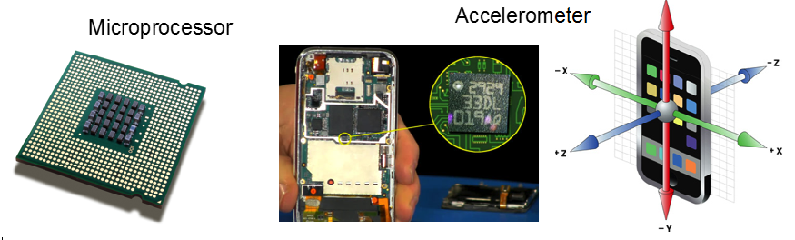
Thin film depositionThin films (< 100 nm) are typical components of modern devices in a variety of fields, including microelectronics, biotechnology and microfluidics. The need for miniaturization and structuration has boosted the development of advanced thin film growth techniques that can be easily implemented in the manufacturing steps of device production. As free-standing structures, two-dimensional thin films have advantages over bulk materials due to their large surface-to-volume ratios, desirable for applications requiring enhanced surface interactions. Thin films can also be employed as coatings over bulk materials to achieve application-specific properties that are unattainable in the substrate material.
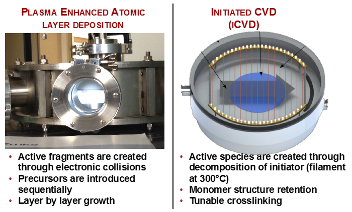
The combination of polymers with inorganics can drive to innovative hybrid functional materials. During the exercise, two Chemical Vapor Deposition (CVD) methods will be used to deposit thin film coatings on different substrates.
The objective of the experiments is to get familiar with thin film growth techniques and understanding the advantages and disadvantages of the different methods. The thin films will be characterized by ellipsometry, to determine thickness and optical properties. |